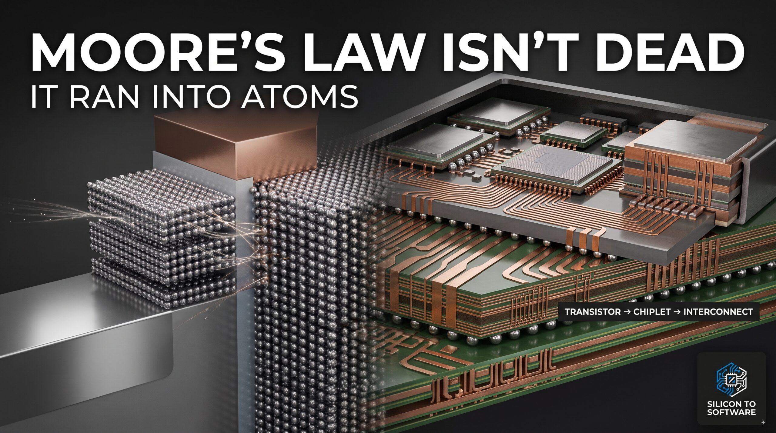
Moore’s Law and Advanced Packaging: Why Chip Scaling Moved From the Transistor to the Interconnect
As lithography approaches atomic-scale limits, chiplets, substrates, and low-loss laminates have become the real engineering battleground for the next generation of performance gains.
Table of Contents
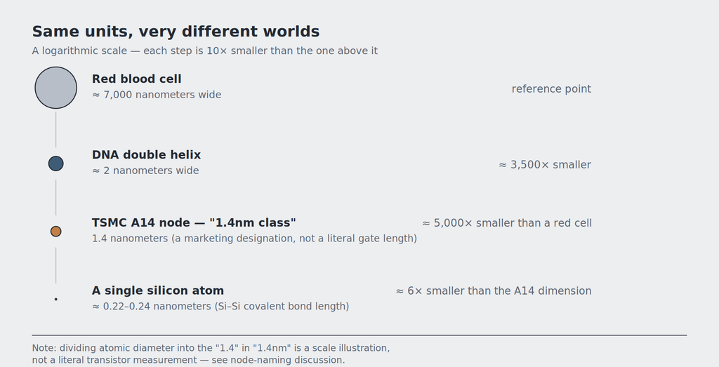
Moore’s Law is running into a wall measured in atoms — literally. A silicon-silicon covalent bond runs about 0.22–0.24 nanometers long. Under the standard touching-spheres convention chemists use to define atomic radius, that bond length is approximately equal to one atom’s own effective diameter — so it puts a single silicon atom at a bit over 0.2 nanometers across. TSMC’s next logic node, A14, is built on a 1.4-nanometer-class process and is scheduled to enter volume production in 2028. Divide one number by the other, and you get transistor features only a handful of atoms wide. That division treats the node number as a physical dimension, which — as the next section explains — it technically isn’t; it’s arithmetic for scale illustration, not an official TSMC figure or a literal transistor measurement, but close enough to establish the scale of the problem the semiconductor industry is now working against.
At that scale, quantum tunneling stops being a rounding error and starts being a design constraint. This is the same physical crisis that forced the industry’s shift to high-k dielectrics and metal gate stacks in the mid-2000s: as SiO2 gate-oxide thickness scaled down toward roughly 1–1.5 nanometers, tunneling probability increased exponentially, and electrons began passing through the oxide barrier even when they lacked the classical thermal energy to cross it. Modern GAA transistors don’t use a literal 1-nanometer conventional oxide anymore — high-k materials allow greater physical dielectric thickness while keeping a much smaller electrical-equivalent thickness — but the underlying tunneling physics hasn’t gone away. It shows up today as source-to-drain tunneling, which now competes with gate leakage as a limiting factor in sub-10-nanometer channel devices.
Here’s what most coverage of this topic misses: the semiconductor industry didn’t stop scaling when it hit that wall. It relocated the fight — from the transistor to the package. This article explains what that shift actually looks like at the engineering level, why it isn’t a free workaround, and which constraint now matters most for anyone designing systems downstream of the fab.
A note on perspective: this analysis comes from the PCB manufacturing and hardware supply chain side of the industry — the substrate, interconnect, and board-level work that consumes whatever the fab produces. That vantage point matters here because the part of this story that gets the least public attention is the part happening below the die.
What “1.4 Nanometer” Actually Means
My first instinct whenever a “next node” headline runs isn’t to ask how small the transistor got. It’s to ask what that number actually measures.
For years now, the honest answer has been: not much, physically.
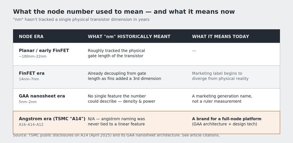
TSMC brands its upcoming generation “A14” — widely reported as an angstrom-referenced designation, following the same convention as its A16 node — rather than a strict “1.4nm” label tied to a specific measured feature. It’s built on second-generation gate-all-around (GAA) nanosheet transistors, per statements from TSMC executives at the announcement and on later earnings calls, not a linear shrink of a planar or FinFET structure. That naming shift is a concrete, citable example of a node name functioning as a marketing convention rather than a literal gate dimension — one data point, not proof of an industry-wide rule, but the clearest one available with a direct source behind it.
This is the single most common error in how this topic gets covered outside the industry: treating the node number as a literal ruler measurement, then treating any slowdown in that number’s shrinkage as proof Moore’s Law has stalled. The number was never a precise physical measurement in the way the public assumes. What’s actually slowing is the rate at which pure lithographic shrink alone can deliver the density and power gains the industry used to get from node transitions during the Dennard scaling era — a narrower, more specific claim than “engineers can’t make chips faster anymore.”
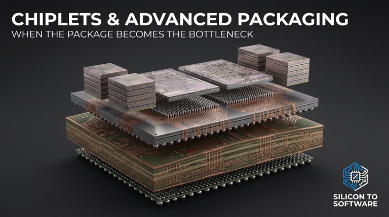
Where Moore’s Law’s Real Density Gains Are Coming From: Advanced Packaging and Chiplets
A14 itself is proof transistor scaling hasn’t stopped — TSMC states more than 20% higher logic density versus N2, a real device-level gain, not a rounding error. But if you want to see where an increasing share of total system-level performance is coming from, the transistor isn’t the only place to look anymore. Look at the package too.
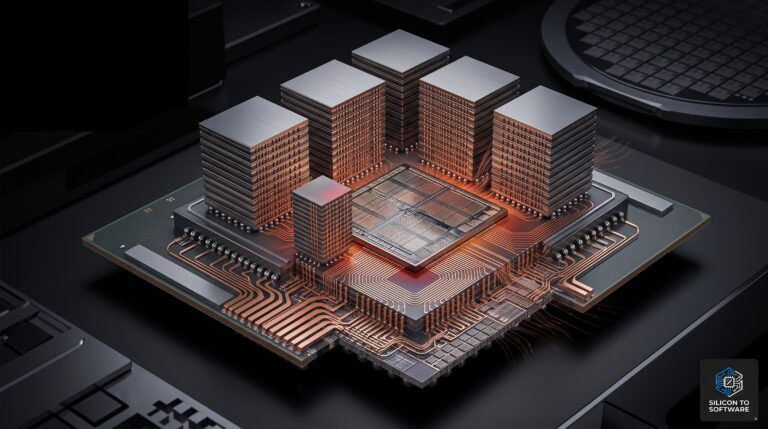
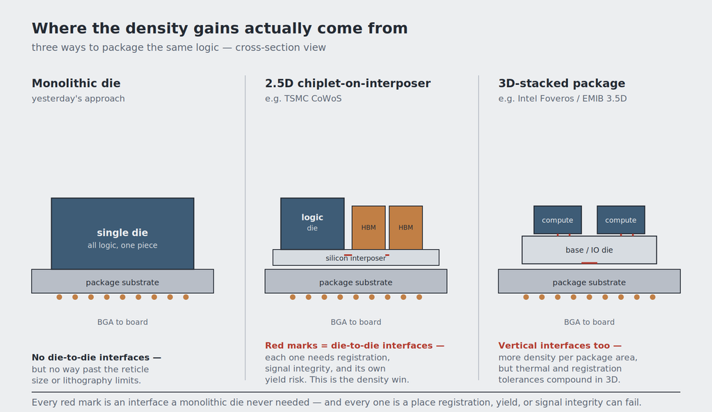
TSMC’s own April 2025 press release lays out exactly what this looks like in practice. Alongside A14, the company detailed plans to bring 9.5-reticle-size CoWoS (Chip-on-Wafer-on-Substrate) to volume production in 2027, enabling integration of 12 or more HBM (High Bandwidth Memory) stacks in a single package alongside leading-edge logic. It also detailed SoW-X, a CoWoS-based system-on-wafer offering the company states delivers 40 times the computing power of its current CoWoS solution, also targeting 2027 volume production. (TSMC’s own CoWoS capacity — not the wafer fab — has been the binding constraint on AI accelerator output for nearly two years; I go deeper on the capacity numbers and the Arizona buildout in TSMC Arizona Bottleneck: A $265B Warning for AI Chips.)
TSMC has kept updating A14’s status since that announcement. At the company’s April 2026 Technology Symposium, TSMC specified A14 volume production for 2028 and announced derivative nodes A12 and A13 for 2029. On its July 2026 earnings call, the company reported an internal test vehicle demonstrating close to 90% device performance and close to 90% 256-megabit SRAM yield.
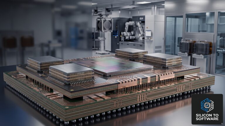
Intel has pursued a parallel path. According to Intel’s own foundry documentation, EMIB (Embedded Multi-die Interconnect Bridge) has been in use since 2017 to embed bridges directly in the substrate and expand beyond a single die’s reticle size limit, without the wafer-level assembly steps a silicon interposer requires. “Foveros” is now a family of Intel heterogeneous-integration approaches rather than one fixed technique: Foveros-S and Foveros-R use silicon or redistribution-layer interposers for 2.5D integration, while Foveros Direct provides true vertical 3D stacking via direct copper-to-copper bonding between dies, without a traditional interposer. Intel has also combined EMIB and Foveros into what it calls EMIB 3.5D — used, for example, in the Intel Data Center GPU Max Series, which Intel describes as its most complex heterogeneous chip in mass production, with more than 100 billion transistors across 47 active tiles spanning five process nodes.
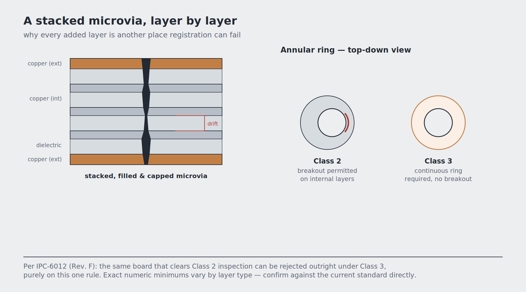
This isn’t fringe engineering — it’s cross-industry infrastructure. AMD, Arm, ASE Group, Google Cloud, Intel, Meta, Microsoft, Qualcomm, Samsung, and TSMC co-developed UCIe (Universal Chiplet Interconnect Express), an open specification for die-to-die interconnect between chiplets from different vendors and different process nodes. The 1.0 specification, released March 2, 2022, already defined a physical layer supporting data rates up to 32 GT/s; version 1.1 followed August 8, 2023; version 2.0 arrived in August 2024, adding 3D packaging support and manageability features; version 3.0 arrived in August 2025, pushing top data rates to 48 and 64 GT/s. That release cadence is itself a signal: ten major semiconductor, cloud, and packaging companies are actively co-engineering the assumption that future performance gains come from how well you connect multiple smaller dies together, not from how small you can make one monolithic die.
Advanced Packaging Isn’t New — Its Centrality Is
A decade ago, 2.5D and 3D integration were far less widespread, concentrated heavily in the highest-end, most expensive networking and server silicon. Today, substrate-like PCB (SLP) and high-density interposer work is being specified for programs that two or three years ago would have used a straightforward 8-layer HDI board — a shift I’ve watched directly from the PCB supply-chain side. That shift didn’t happen because packaging got easier. It happened because packaging became the more economical place to keep extracting performance, relative to the cost and yield risk of continuing to chase pure transistor shrink at the bleeding edge.
That shift also moved the hardest unsolved problem in the stack somewhere new — off the transistor and onto the interconnect between chiplets. (For a deeper dive into why substrate and interposer capacity — not the chiplets themselves — is the actual manufacturing bottleneck, see Chiplets and Advanced Packaging: Why Substrate Capacity Is the Real Manufacturing Bottleneck.)
The Overlooked Bottleneck: PCB and Substrate-Level Interconnect Engineering
Connecting multiple chiplets doesn’t eliminate the scaling problem. It relocates it — to the interconnect level, which is squarely PCB and substrate territory.
Specification. A chiplet package needs a substrate — and often a board underneath it — capable of routing an enormous number of high-speed signals in a tight footprint, with controlled impedance and low insertion loss, out to the rest of the system.
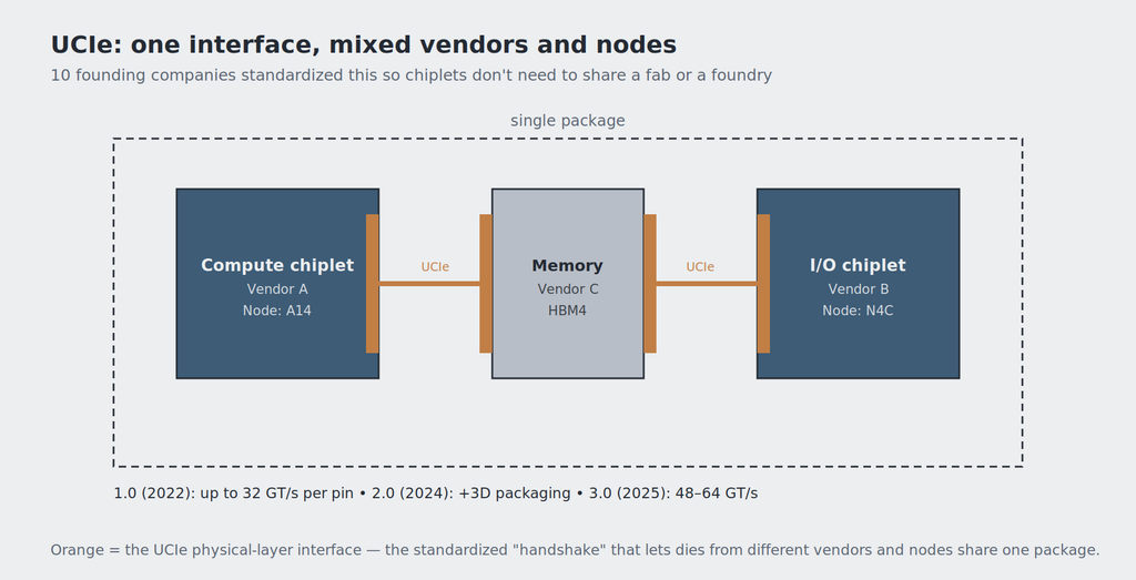
Mechanism. To hit that routing density, fabricators lean on microvia structures — stacked, filled, and capped vias drilled with lasers rather than mechanically — to route signal layers that a standard through-hole via geometry can’t reach. Every additional stacked microvia layer adds another interface where layer-to-layer registration has to hold. IPC-6012, currently in Revision F, is the qualification and performance specification for rigid printed boards, published alongside IPC-6011A (which defines the Class 1/2/3 performance classes) and IPC-A-600M (visual acceptance criteria).
What “materially tighter” means in practice: multiple independent industry sources consistently describe Class 2 as permitting 90-degree annular-ring breakout on internal layers under defined conditions, while Class 3 does not allow breakout at all — every via has to retain a continuous ring of copper around the drilled hole. That single rule is why a board that passes Class 2 inspection can still get rejected outright at Class 3. Exact numeric annular-ring minimums vary by layer type and which edition’s table is cited, so specifiers should confirm exact figures against the current IPC-6012 revision directly rather than a secondary summary.
Trade-off. Every increase in routing density — finer line/space, tighter pitch, additional stacked microvia layers — trades against manufacturability and yield. This is the same shape of trade-off the industry has fought at the lithography level for two decades, just relocated — and it doesn’t relocate to one single point of failure. Advanced-packaging yield risk spreads across die fabrication, bump and bonding defects, interposer/RDL routing, substrate fabrication, assembly, and test. From the board and substrate side specifically, laser-drill registration accuracy and copper-fill reliability are the pieces of that broader picture I watch most closely — but they’re one contributor to a larger yield problem, not the whole of it.
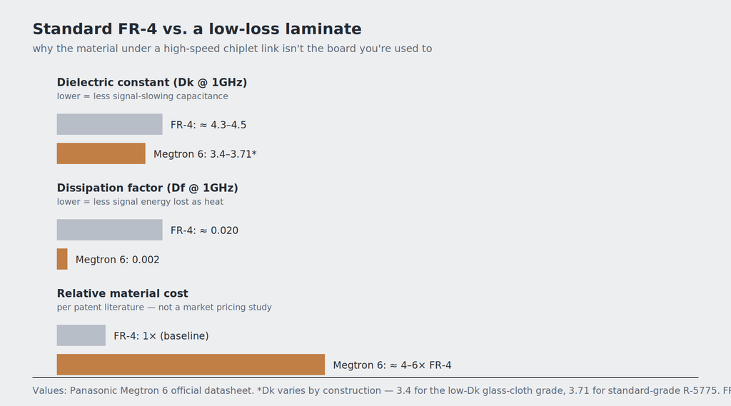
Practical consequence. A world-class die can be strangled by a substrate that can’t route its ball-out cleanly, or by a board stackup that introduces enough fiber-weave-induced skew to blow a timing budget on a high-speed SerDes lane. Conventional, higher-loss FR-4 systems can eat up too much of the insertion-loss budget on long or very-high-speed channels — how much is too much depends on channel length, signaling rate, and stackup, not on FR-4 as a category being categorically unusable — which is why designers increasingly move to lower-loss laminates like Panasonic’s Megtron 6 for the highest-speed layers. Per Panasonic’s own datasheet, standard-grade Megtron 6 (R-5775) runs a dielectric constant around 3.71 at 1 GHz; the low-Dk glass-cloth variant (R-5775(N)/(K)/(G)) comes in lower, at 3.4. Both carry a dissipation factor of 0.002 at 1 GHz and a thermal decomposition temperature of 410°C — exact numbers depend on which specific construction and glass style you’re speccing. (For a full construction-by-construction comparison against Megtron 8 and Isola’s Tachyon 100G — including where the datasheet headline number quietly misleads you — see Choosing the Right High-Speed Laminate for AI Hardware.) Low-loss laminates carry a real cost premium over standard FR-4 — patent literature puts one estimate at roughly 4 to 6 times — though the actual delta depends heavily on resin system, copper type, glass style, supplier, and volume, and shouldn’t be read as a fixed market benchmark.
The point isn’t that any single one of these numbers is exotic. It’s that engineers trained in the “transistor is king” era instinctively push complexity down into silicon, because that’s where their training told them the leverage lived. That’s no longer automatically true. Sometimes the cheapest, fastest performance win left on the table is a better dielectric, a rotated glass weave to reduce fiber-weave skew, or a smarter via structure — not another silicon mask revision.
Why Advanced Packaging Isn’t a Free Workaround
Advanced packaging and interconnect-level scaling are not shortcuts around the atomic-scale wall. They’re a different, and in several respects harder, engineering problem. Stacking multiple dies and routing them through an interposer and substrate compounds tolerance stack-up across more interfaces than a monolithic die ever had to manage. Registration risk, thermal management across dissimilar materials, and signal integrity budgets all get harder to close as you add layers and interfaces, not easier.
Look at what TSMC itself is targeting for 2027: a single CoWoS package integrating 12 or more HBM stacks alongside leading-edge logic. Each of those stacks adds routing, bonding, and thermal complexity across the interposer/RDL and substrate hierarchy — more microbump and other package-level bonding interfaces that have to register correctly, more thermal boundaries between dissimilar materials, more high-speed signal paths that have to survive the trip across the package.
A monolithic die doesn’t carry that particular burden, because it doesn’t have inter-die interfaces at all — it still has its own package-level interfaces (bumps, substrate connection, thermal boundaries), just not the die-to-die kind. The cost structure reflects the added difficulty: low-loss laminates alone carry a real premium over standard FR-4 (patent literature cites roughly 4–6x, though the real number varies by supplier and volume), and that’s before accounting for the added process steps advanced packaging requires.
Chiplet integration also carries a yield-multiplication problem a monolithic die never faced. If several individually tested chiplets each yield in the mid-90% range, a packaged assembly’s effective yield compounds downward unless every chiplet is pre-screened with known-good-die (KGD) testing before final assembly. Synopsys’s own published chiplet design guidance recommends exactly this practice. But that screening reduces the risk — it doesn’t eliminate it. A die can pass its own test and still contribute to a failed package if bonding, interposer, or assembly defects show up afterward, so KGD testing adds real cost without fully removing the compounding-yield problem it’s meant to address.
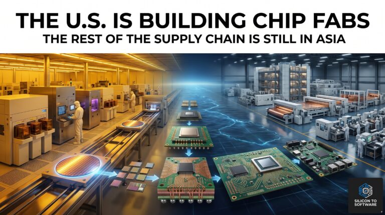
Two things this article deliberately doesn’t resolve, worth flagging rather than glossing over: multi-vendor chiplet integration raises a hardware trust question — how do you verify a die from another company’s fab hasn’t been tampered with before it’s sealed permanently into your package — that’s a live, unresolved discussion in the chiplet ecosystem. And this piece shouldn’t imply a geographic risk it hasn’t actually checked: TSMC’s CoWoS and SoW-X capacity is heavily concentrated in Taiwan, a real supply-chain concentration risk worth its own separate treatment — but Intel’s own newsroom describes EMIB and Foveros advanced-packaging operations running in the United States (New Mexico) as well, so folding all four technologies into one “built in Taiwan” claim would overstate the case. The concentration risk is real; it’s just not evenly distributed across every technology named here.
That doesn’t make this path a failure. It makes it an honest trade — a more difficult, more expensive, lower-yield path than shrinking a transistor used to be.
The Constraint Engineers Should Watch
If you’re designing systems in this environment, the constraint that will most often decide whether your architecture’s theoretical performance is actually reachable isn’t transistor density anymore. It’s interconnect density and the signal integrity budget available to support it — how many high-speed signals you can move on and off a die, through an interposer, across a substrate, and onto a board, at the bandwidth your system needs, without exceeding your loss budget or blowing your timing margin.
The most advanced die in the world is only as fast as the package and board underneath it. If those can’t get signals in and out fast enough and clean enough, the transistor-level cleverness never reaches the system level.
Silicon didn’t stop shrinking because engineers ran out of ideas. It stopped shrinking easily because it ran into the size of atoms — and the industry answered by moving the problem to the package. Moore’s Law isn’t dead. It just moved — and that’s the half of the scaling story most coverage still leaves out.
About the Author
Imran Valiani | Sales Director, PCB Electronics Manufacturing
20+ years working with major Bay Area and global tech clients. Founder of Silicon to Software, where I write about the hardware layer — PCB fab, AI gear, autonomous systems, and cyber — the stuff most tech writers have never touched. Literally.
Follow: X @SiToSoftware | LinkedIn
This post was written with AI assistance. See my full AI disclosure.
Sources and Further Reading
Primary sources (company/organization statements) are marked accordingly; others are trade press reporting on those statements.
- TSMC, “TSMC Unveils Next-Generation A14 Process at North America Technology Symposium,” April 2025 — primary
- TSMC, “A16 Technology,” official technology page — primary
- Tom’s Hardware, “TSMC confirms significant yield and performance improvements in A14 update,” July 2026 — reported, quoting TSMC’s CEO on an earnings call. The underlying remarks are independently corroborated verbatim across seven financial-transcript services (Motley Fool, Globe and Mail, Investing.com, Benzinga, Yahoo Finance, Webull, SahmCapital); TSMC’s own PDF transcript could not be directly fetched (bot detection) — see verification table
- Tom’s Hardware, “TSMC unveils process technology roadmap through 2029,” April 2026 — reported, quoting TSMC’s SVP at a company event
- Intel Foundry, “Advanced Packaging,” official product page — primary
- Intel Newsroom, “Intel’s U.S. Advanced Packaging Enables Next-Generation AI Semiconductors,” July 2026 — primary
- UCIe Consortium, “Press Releases,” official specification release history — primary
- IPC, IPC-6012 product listings, Association Connecting Electronics Industries — primary (catalog metadata only; full standard text not independently reviewed)
- Dudek & Hart (Compunetics Inc.), “The Enigmatic Breakout Angle,” hosted on IPC’s document server — technical paper confirming Class 1/2/3 breakout-angle definitions
- Bhattacharyya, “A Compact Model of Silicon-Based Nanowire Field Effect Transistor,” arXiv — source for the 90nm-node gate-oxide tunneling figures
- Intel, “High-K Gate Dielectrics for CMOS Transistors,” white paper — independent primary corroboration of the same 90nm/1.2nm oxide figures
- Panasonic Industrial Devices, “MEGTRON 6 Family of PCB,” official datasheet — primary
- Synopsys, “Chiplet Design Best Practices for Multi-Die Systems,” design guidance on known-good-die testing — primary (vendor technical guidance, not an independent standards body)