
Industrial IoT Hardware Reliability: Why Boards That Pass Lab Testing Still Fail on the Factory Floor
Thermal cycling, connector fretting, moisture, and electrical noise turn ordinary design decisions into industrial failure modes — here’s the engineering behind each one.
Table of Contents
A board came back to us nine months after it shipped. It had cleared full functional test. It had cleared EMC pre-compliance. Every engineer who signed off on that design review would tell you, correctly, that the board worked.
It failed anyway — a hairline crack at the corner of a BGA package, invisible until a thermal camera and a cross-section showed exactly where the joint had opened. The board hadn’t been damaged. It had been used in an environment that ran it through more thermal cycles in a year than the lab test plan had run through in its entire qualification.
A board that fails on a factory floor often passed its functional test first. That’s not a contradiction — it’s the core industrial IoT hardware reliability problem this piece exists to explain. A standard time-zero functional test proves a circuit works at the moment you run it; by itself, it doesn’t establish whether that circuit survives thermal cycling, vibration, electrical noise, moisture, and continuous duty for years — those require separate environmental and accelerated-life testing that many functional test plans don’t include.
Those are different engineering questions, and failures happen when teams validate time-zero function without adequately validating the deployment environment it’s actually headed for. Twenty years of watching field returns come back into PCB manufacturing facilities has made the pattern hard to miss: the gap almost never sits in the schematic. It sits in the decisions made — or skipped — before the board was ever laid out.
This piece covers the physical and environmental reliability layer — the mechanical and material engineering that determines whether hardware survives its deployment environment. It doesn’t cover hardware security (secure boot, firmware integrity, supply-chain trust) or hazardous-area/functional-safety certification (ATEX/IECEx, IEC 61508); both deserve their own treatment, and neither is addressed here.
This piece walks through the specific engineering mechanisms that separate a board that survives industrial deployment from one that only survives the lab: thermal cycling and solder fatigue, connector fretting, moisture and corrosion, EMC/EMI susceptibility, component derating, enclosure thermal design, and maintainability — and where the line actually sits between reliability engineering and over-engineering.
It’s the same underlying problem I flagged as an open gap when I wrote about the hardware bottlenecks holding back humanoid robots on the factory floor — that piece noted PCB reliability standards were out of scope there and promised a dedicated follow-up. This is that follow-up.
What “Industrial-Grade” Actually Means for Industrial IoT Hardware
“Industrial-grade” gets treated as a label — swap in a wider-temperature-range part, spec a sealed enclosure, done. It isn’t a component swap. It’s a set of decisions made at the material and stackup level, before layout is locked, that determine whether the board can absorb years of environmental stress without degrading.
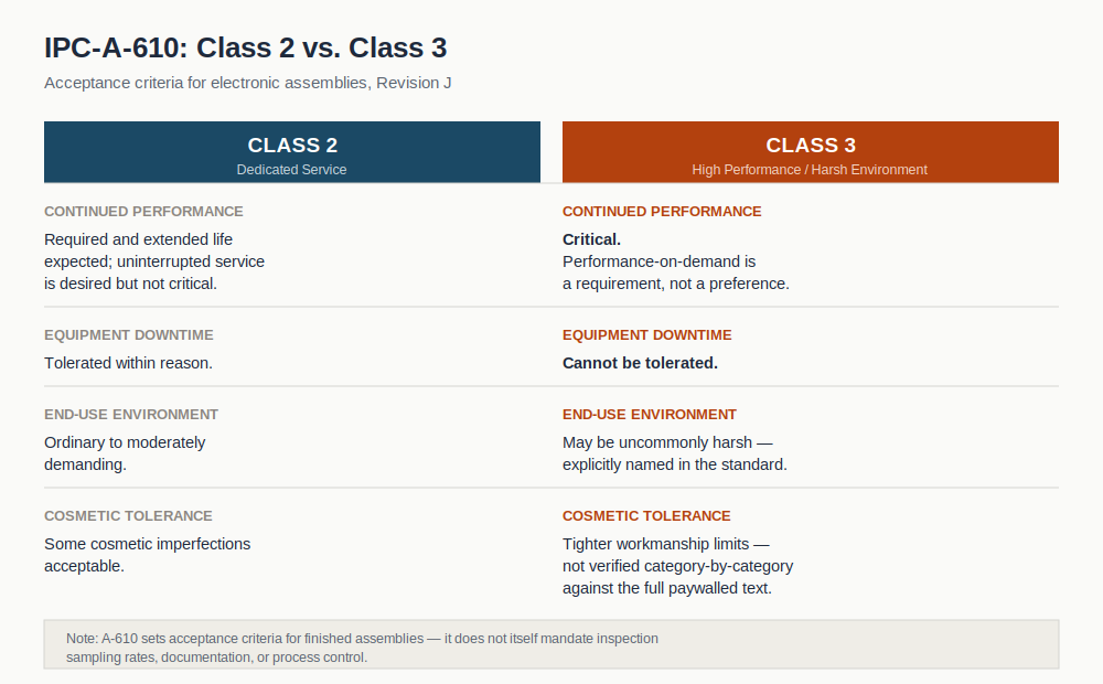
IPC-A-610, currently at Revision J, defines three acceptance classes for electronic assemblies. Class 2 covers “dedicated service” products where continued performance and extended life are required and uninterrupted service is desired but not critical, with some cosmetic imperfections acceptable. Class 3 covers what IPC terms “High Performance/Harsh Environment Electronic Products” — continued performance or performance-on-demand is critical, equipment downtime cannot be tolerated, and the end-use environment may be uncommonly harsh.
Where A-610 sets class-specific acceptance criteria, Class 3 generally applies tighter limits than Class 2 — though I’d stop short of claiming that holds category-by-category across the entire standard, since the full published text sits behind IPC’s paywall. Worth being precise about what A-610 itself governs: it’s an acceptability standard for finished assemblies, not a mandate for inspection sampling rates, documentation levels, or process controls — those come from the applicable contract, quality system, and companion standards like J-STD-001, layered on top of whichever class you specify.
My interpretation, from two decades of watching field returns: in many of the programs I’ve encountered, hardware marketed as “industrial” is built to Class 2 assumptions with an industrial label added afterward. That gap between the marketing claim and the actual specified class is where a lot of these failures start.
If your purchase order, assembly drawing, or governing quality documentation doesn’t identify an applicable workmanship or acceptance standard and revision, the acceptance basis is ambiguous — you’re relying on whatever the shop floor assumes, not on something you specified. For a sense of what the far end of this spectrum actually looks like in practice, satellite PCB programs run to IPC-A-610 Class 3 plus a space-specific addendum — a useful contrast for seeing how much further the acceptance bar moves once field service isn’t an option at all.
Thermal Cycling and Solder Fatigue: The Mechanism Behind Field Failures
Solder is not a permanent bond. It’s a wear-out material.
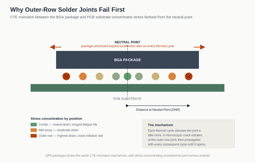
Every time a board heats up and cools down, the PCB substrate and the component package expand and contract at different rates — a coefficient of thermal expansion (CTE) mismatch. That mismatch concentrates mechanical stress at the solder joints connecting them, most severely at the outer-row joints of BGA packages, which sit farthest from the neutral point of expansion. QFN packages face the same underlying CTE-mismatch mechanism, not a different one — peer-reviewed thermal cycling research on QFN packages finds peak strain energy density concentrated at the top corner of the peripheral solder joints, driving fatigue failure there.
What changes with QFN geometry is where that stress concentrates and what else influences it: standoff height, pad and package dimensions, and the center thermal pad’s solder attachment all shift the fatigue-life outcome, and pad cratering and thermal-pad voiding are real, separate concerns worth designing against — but they sit alongside classic solder-joint fatigue, not in place of it.
IPC-9701B, the current revision, establishes the thermal cycling test method used to characterize the fatigue lifetimes of surface-mount solder attachments, with results intended to support predictions of field lifetime for a given use environment. Under this methodology, fatigue life is typically reported as a Weibull “characteristic life” — the cycle count at which 63.2% of a test population has failed — which is a specific statistical parameter, not a simple average or a guaranteed minimum.
One caveat the standard itself is careful about: accelerated-cycle counts aren’t a direct stand-in for field years. Solder creep and stress relaxation are time-dependent, so translating lab cycles into calendar time requires an appropriate acceleration factor, not a 1:1 reading of the number.
A study published in Nature Communications — Xian, Xu, Stoyanov, Coyle, Dunne, and Gourlay, 2024, a collaboration between Imperial College London and Nokia Bell Labs — thermally cycled 32 BGA packages from 0°C to 100°C at 10°C per minute with 10-minute dwells at each extreme, following IPC-9701A guidelines, and found a Weibull characteristic life (N63.2) of 7,286 cycles before failure. A separate finite-element simulation by Lee et al. — cited within a 2022 ScienceDirect study on BGA solder joint microstructure evolution — modeled a wider swing (-40°C to 125°C) and predicted thermal fatigue lives exceeding 3,000 cycles.
These aren’t a controlled comparison: they involve different packages, alloys, test conditions, and methodologies, so the numerical cycle counts shouldn’t be compared directly against each other. The broader thermomechanical fatigue literature independently establishes the underlying point: fatigue life generally declines as cyclic strain and thermal-cycling severity increase.
Xin Wei’s doctoral dissertation at Auburn University, reviewing solder joint fatigue research, found that characteristic fatigue life consistently decreases as strain level or thermal-cycling severity increases, because the joint accumulates more damage on every single cycle. That relationship is what a design’s thermal cycling range actually costs when it’s treated as an afterthought instead of a spec.
The mechanism is straightforward and unforgiving: repeated CTE-driven stress cycles the solder joint until a microscopic crack initiates, then propagates a little further with every cycle, until the joint opens. That strain-based description is the standard entry point into the mechanism; current solder reliability research increasingly favors energy-based models (creep strain energy density) as more accurate than pure strain-range approaches, though the underlying driver — repeated CTE mismatch loading the joint — is the same physical starting point either way.
The trade-off is that higher-reliability laminate choices carry their own cost and electrical-material trade-offs — different resin systems, Dk/Df, and fabrication characteristics come bundled with better CTE matching and higher glass transition temperature (Tg), even though Tg itself doesn’t directly govern impedance or dielectric loss.
The consequence is about timing, not magnitude — these failures don’t show up at time zero. They show up once enough cycles have accumulated, and it’s specifically frequent power-cycling or process-driven temperature swings — not continuous operation at a stable temperature — that accumulate those cycles fast; a board running 24/7 at one steady temperature can rack up far fewer damaging thermal cycles than one that powers on and off, or tracks a batch process, several times a day.
A design that never runs a thermal cycling test to a profile matching its actual deployment environment is making an assumption about that number, not a verified claim.
Connector Fretting: Two Drivers, Not One
Vibration causes a failure mechanism I’ve seen misdiagnosed more often than almost anything else in this business — and it’s worth being precise about what actually drives it, because it isn’t only vibration.
A peer-reviewed study — Flowers et al., IEEE Transactions on Components and Packaging Technologies, 2004 — running single-frequency vibration tests on tin-alloy-plated contacts found threshold behavior: below a given g-level at a given frequency, fretting degradation doesn’t meaningfully progress; above it, similar g-levels produce similar fretting rates. That accounts for the externally driven half of the mechanism.
The other half doesn’t need vibration at all. Connector manufacturer technical documentation from Smiths Interconnect points out that thermal cycling itself — independent of any external vibration source — causes fretting, because differential expansion and contraction between mating surfaces produces micro-movements at the contact point, and that non-noble platings like nickel oxidize faster as temperature rises.
A separate technical note from Samtec makes the same point from a different angle: thermal motion in the contacts, standoffs, housings, and heat sinks around a connector causes fretting on its own, and the resulting motion isn’t confined to one axis — it can be radial, axial, or transverse.
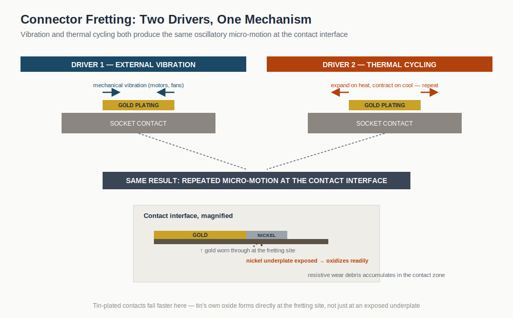
Combine the two, and a board sitting in a sealed, thermally cycling enclosure can develop connector fretting with zero external vibration at all, purely from its own thermal expansion. Add real mechanical vibration from nearby motors or fans, and the two failure paths compound rather than substitute for each other.
The motion wears through the plating and exposes the base metal underneath to oxidation. Contact resistance climbs gradually, then intermittently, then fails outright — often correlating with a thermal cycle that briefly opens an already-degraded contact. The specific chemistry matters here: tin-plated contacts are especially vulnerable because tin forms an insulating oxide directly at the fretting site, and the wear process generates resistive debris that accumulates in the contact zone.
Gold resists oxide formation almost entirely, which is why gold-plated contacts outperform tin in vibration-prone applications — not simply plating thickness. In gold-plated designs, the exposed base metal that eventually oxidizes is usually a nickel underplate sitting beneath the gold, not nickel used as the mating surface itself — nickel oxide is highly resistive, which is exactly why it’s buried under gold rather than left exposed in the first place.
The symptom looks exactly like a software bug: intermittent, non-reproducible on the bench, worse under conditions nobody can quite pin down. I’ve watched firmware teams spend weeks chasing that ghost before someone pulls the connector and finds the wear pattern under a microscope.
Connectors with heavier gold plating and higher contact normal force resist fretting better, up to a point — more plating and more force aren’t free upgrades. Excessive normal force increases friction, wear, and insertion force, and can itself accelerate mechanical damage, so this is a real engineering trade-off to tune, not a dial to max out.
It costs more and may need a different footprint either way — exactly the kind of trade-off that gets quietly decided by a BOM cost target rather than a vibration and thermal profile. And because the failure can originate from the board’s own thermal cycling rather than an obvious external vibration source, field diagnosis usually takes longer than diagnosing the original mechanical problem would have, because nobody suspects the connector first.
Moisture, Condensation, and Corrosion in Sealed Enclosures
Uncontrolled thermal environments create condensation cycles. When a board’s temperature drops below the local dew point — which happens routinely in unheated enclosures exposed to daily thermal swings — moisture condenses directly onto exposed conductors.
That moisture film becomes a conductive electrolyte path. Given closely spaced conductors under bias, it can drive electrochemical migration or corrosion, both of which degrade insulation resistance slowly, long before they cause a hard short.
In practice, that decline doesn’t announce itself. It shows up as sensor drift that tracks with weather rather than with anything in the process being measured, or as noise on an analog line that appears on humid mornings and disappears by afternoon — symptoms that get chased as calibration or firmware problems for months before anyone traces them back to a corroding trace.
Conformal coating, qualified under IPC-CC-830C, is intended to provide protection from moisture and contamination and to provide electrical insulation — but the standard itself is explicit that coating is not intended as a sole source of mechanical support. That distinction matters more than it sounds: coating protects the board surface, but it doesn’t stop moisture from accumulating inside a poorly sealed enclosure in the first place, and how well it protects even the surface depends heavily on coating chemistry, thickness, coverage, and application quality — it’s not a uniform guarantee.
Ingress protection ratings under IEC 60529 describe what an enclosure actually excludes — a two-digit code for solid-object and water ingress, tested against a defined set of laboratory conditions.
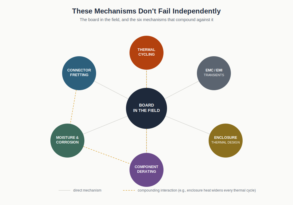
Moisture ingress and wide thermal swings often coexist in outdoor or poorly controlled industrial installations rather than sharing one single root cause — but where they do coexist, a board with a marginal IP rating isn’t just facing corrosion risk in isolation; it’s facing corrosion acting simultaneously with the CTE-driven solder fatigue described above.
EMC/EMI, Transients, and Power Supply Robustness on the Factory Floor
A factory floor’s electrical environment is not a clean bench. Motor drives, contactors, and relays generate conducted and radiated noise, along with fast transients, that a consumer EMC pre-compliance scan often doesn’t test for at all. That’s not because the physics can’t be reproduced in a lab — standardized test generators exist specifically to replicate these disturbances without needing an actual motor or contactor present. The real gap is testing to inadequate severity levels, skipping the relevant immunity tests, or running an emissions-only scan and calling it “EMC pre-compliance.”
The IEC 61000-4 series defines the test methods: 61000-4-2 (currently Edition 3.0, published March 2025) for electrostatic discharge immunity, 61000-4-4 (Edition 3.0, 2012) for electrical fast transient/burst immunity, and 61000-4-5 (Edition 3.0 from 2014, amended in 2017; the consolidated version is Edition 3.1) for surge immunity.
But the test method alone doesn’t tell you what severity level applies — that’s set separately by IEC 61000-6-2, which governs immunity requirements for industrial equipment where no dedicated product-specific or product-family EMC standard already takes precedence. A product tested to 61000-4 methods at residential or light-commercial severity levels hasn’t been tested to an industrial standard, even though the test names look identical.
The mechanisms themselves are physically distinct. Electrical Fast Transient (EFT)/Burst reproduces the repetitive fast transients generated by switching inductive loads — relays, contactors, motors — as pulses in the nanosecond range repeated in bursts. Surge testing applies longer-duration, higher-energy transient waveforms associated with switching events and indirect lightning strikes, via specified waveforms and coupling networks rather than a single simple pulse.
Without protection appropriate to the interface and expected transient energy — which might mean TVS diodes, filtering, isolation, or proper grounding and return-path design, depending on the port — a product that passed EMC pre-compliance in a quiet lab can still reset, corrupt data, or degrade internally when a nearby motor drive cycles.
This is the pattern that shows up as a support ticket instead of a field return. The board resets, always around the same time of day, always when a particular piece of equipment nearby switches on. Nobody suspects the electrical environment first, because the product passed EMC pre-compliance — on a bench that never had a contactor anywhere near it.
Where Margin Actually Disappears: Component Derating in Practice
Component derating — operating parts below their rated voltage, current, or thermal limits — is the design-review control that catches marginal component selection before it becomes a field failure. It’s also the easiest control to quietly erode under BOM cost pressure, because the effects don’t show up in functional test. It’s the same category of problem as the DFM mistakes that quietly erode fabrication yield — an annular ring breakout on a Class 3 board, for instance, can contribute to exactly the kind of long-term thermal-cycling reliability risk this piece is about, not just an immediate fabrication defect.
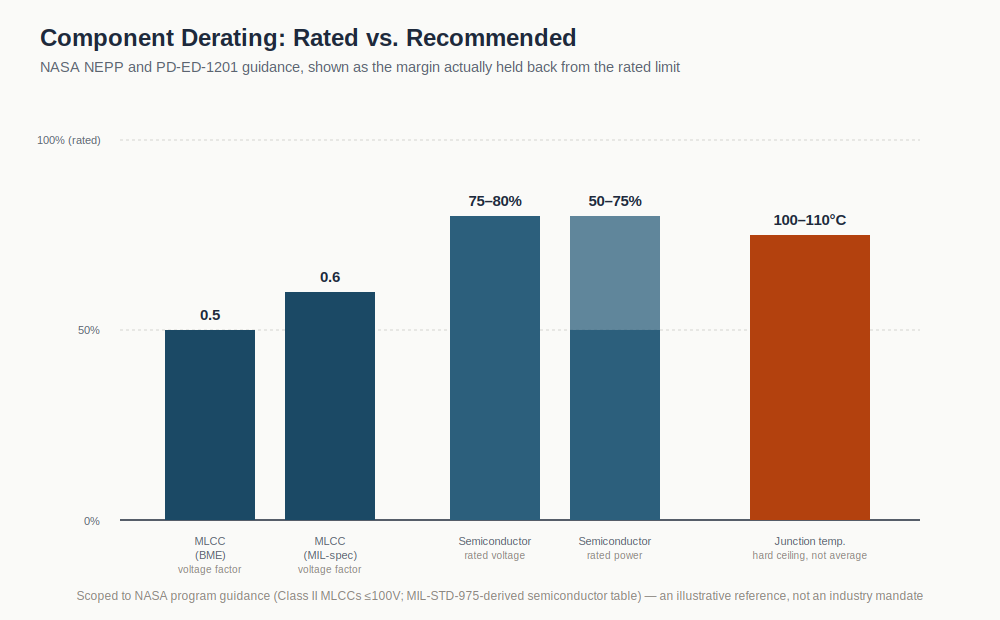
For ceramic capacitors, a NASA technical presentation on MLCC reliability (2013, scoped to Class II MLCCs ≤100V) gives concrete derating guidelines: a voltage derating factor around 0.5 for base-metal-electrode parts and around 0.6 for MIL-spec parts, with the presentation concluding that 50% voltage derating “seems reasonable.” Over-derating isn’t free either — choosing a larger case size purely to get a higher voltage rating at the same capacitance can make the part more susceptible to mechanical fracture. Derating has a floor and a ceiling.
For semiconductors and other active parts, NASA’s own preferred reliability practices (PD-ED-1201) set derating levels by part class — 75–80% of rated voltage, 50–75% of rated power, junction temperature ceilings in the 100–110°C range, depending on part type.
Those specific figures trace to MIL-STD-975, NASA’s historical standard parts list — though it’s worth being direct about its status: MIL-STD-975 was formally canceled in 1998, without replacement, so PD-ED-1201’s Table 1 numbers ultimately point back to a document that’s no longer an active standard. They’re not built on MIL-HDBK-217, which is a separate, alternative route to derating via reliability-prediction math, and its underlying statistical methodology is itself contested in the reliability community today; physics-of-failure approaches are increasingly preferred.
Treat the percentages above as a solid illustrative reference point from a high-reliability space program, not an industry mandate. NASA’s EEE-INST-002 is the document typically cited as the current GSFC derating instruction — NASA’s own page identifies it as the April 2008 version (incorporating an addendum to a base document from 2003) and calls it the latest official release, though NASA’s own internal presentations have separately flagged it as needing revision. Treat it as the standing reference, not something recently refreshed.
Within its own program guidance, the source is direct about the consequence of ignoring the limit: maximum junction temperature should not be exceeded at any time, under any condition — not as an average, as a hard ceiling.
Several of the mechanisms above compound when the part underneath them was never given the margin to absorb it. A component running near its rated limit degrades faster under thermal cycling, tolerates transient events worse, and has less headroom against the everyday electrical noise of an industrial environment — though derating doesn’t touch every mechanism in this piece equally; it has little to say about connector fretting from external vibration or moisture ingress through a poorly sealed enclosure.
The Decisions That Happen Before Layout: Stackup, Materials, and Enclosure Thermal Design
Everything above traces back to choices made before the board is even laid out: laminate selection, stackup, and enclosure thermal design. Laminate selection carries its own set of trade-offs even outside a thermal-cycling context — Dk, Df, and manufacturability considerations that stack on top of, not instead of, the CTE and Tg factors covered earlier in this piece.
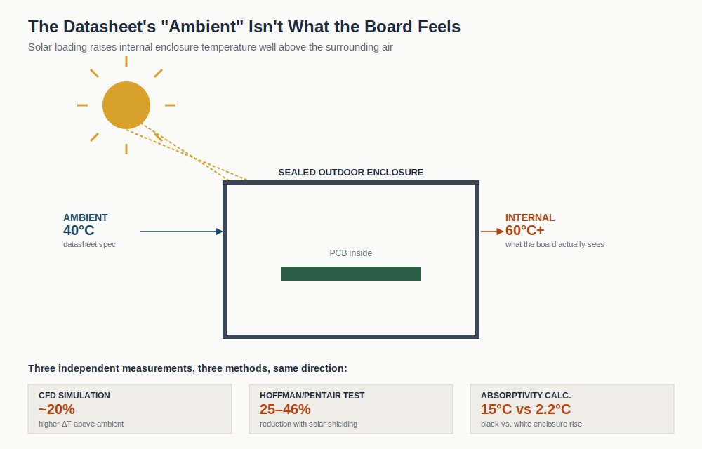
The enclosure matters as much as the board. A CFD simulation of outdoor electronics enclosures found solar loading increased internal temperature rise above ambient by roughly 20% versus the same enclosure without sun exposure — specific to that simulation’s geometry and finish. A Hoffman/Pentair manufacturer test on identical light-gray (RAL 7035) outdoor enclosures points the same way: solar shielding reduced temperature rise above ambient by roughly 25% with a top shield and roughly 46% with top-and-side shielding, for that specific enclosure configuration — a real, if narrow, physical test rather than a generic industry figure.
A third data point is older and worth describing precisely rather than the way I originally framed it: older IEEE guidance (predating the current C37.24) used an approximate 15°C solar-driven temperature rise for black or dark-painted enclosures and derived a corresponding figure of roughly 2.2°C for white enclosures using published solar-absorption coefficients — black around 0.97, white around 0.14. That’s a calculation from absorptivity data, not a field measurement of two identical enclosures side by side, and I’d stated it as the latter in an earlier draft; correcting that here.
The underlying physics — dark surfaces absorb far more solar radiation than light ones — is exactly what those coefficients quantify, and it hasn’t changed. The curren,t reference for this today is IEEE C37.24, board-approved by the IEEE Standards Association on December 10, 2025 and published June 19, 2026, which supersedes the older guidance this kind of calculation was built on. Worth flagging its actual scope, too: C37.24 is specifically a guide for outdoor metal-enclosed switchgear, bus, and control switchboards — useful for the underlying physics, not a general industrial IoT enclosure standard.
A simulation, a physical shielding test, and this older absorptivity-based calculation point the same direction rather than confirming one shared number: solar loading is a real, double-digit factor on enclosure interior temperature, however you measure it. An enclosure’s thermal resistance sets the board’s actual operating temperature, and a sealed, unvented enclosure in direct sun can widen the effective thermal cycling range the solder joints experience well beyond what the ambient spec implies.
Telcordia’s GR-487, a standard originally developed for telecom outside-plant equipment cabinets, illustrates how a real specification tests for exactly this gap: it defines a solar-load test method that illuminates an enclosure from multiple sides at a controlled radiant intensity while internal electronics are powered, then measures the resulting internal temperature rise. It’s telecom-specific in origin and shouldn’t be cited as a general industrial IoT requirement, but the methodology ;s a good illustration of the underlying discipline: measure the real internal temperature under real solar load, don’t assume the datasheet ambient number applies.
A precision worth holding onto here: a 20% increase in internal temperature rise above ambient is not automatically the same as a 20% wider thermal cycle. What solar loading reliably does is push up the peak, daytime side of the cycle — whether that also widens the full hot-to-cold swing depends on the nighttime low and the equipment’s duty cycle, which the CFD study alone doesn’t establish.
Either way, that added peak temperature makes every thermal cycle described earlier in this piece more severe than the datasheet ambient spec implies. The enclosure decision and the solder joint fatigue decision are, mechanically, related decisions — made at two different desks that rarely talk to each other.
Maintainability Is a Reliability Feature, Not an Afterthought
In a 24/7 environment, how quickly a failure can be diagnosed and repaired is a maintainability metric — a distinct discipline from reliability, though the two combine directly into system availability. It’s not a service-department afterthought.
MIL-HDBK-472, the DoD’s maintainability prediction handbook, has made this case since the 1960s and is still listed active: maintainability should be predicted and designed for early, tied directly to a design’s diagnostic and isolation capability and to whether components are built for replacement rather than fixed in place. A more recent academic study on maintainability-focused design reached the same conclusion by a different route — modularity, accessibility, and ease of assembly and disassembly are the physical design attributes most directly linked to reducing mean time to repair, because they’re the direct mechanical enablers of a fast, clean intervention.
Accessible test points, field-replaceable connectors, and basic diagnostic status reporting reduce mean time to repair. In a process running 24/7 without redundancy or bypass capability, that’s not a convenience — every hour a board is down is an hour the line isn’t. Systems with hot spares or redundant paths absorb this better, but many cost-sensitive industrial IoT nodes aren’t designed with that kind of redundancy.
When Full Industrial-Grade Design Isn’t Necessary
Not every industrial IoT deployment needs the full weight of this article. A sensor node inside a climate-controlled cabinet, or a short-lifecycle pilot deployment, may genuinely be well served by consumer-grade design margins. Over-building has real costs too. Meeting Class 3 acceptance criteria can increase manufacturing and quality-assurance cost — tighter workmanship tolerances usually push toward heavier inspection, more rework, and more documentation in practice, even though A-610 itself doesn’t mandate those specifically; they’re the practical consequence of the quality system most organizations build around a Class 3 commitment.
Exactly how much that adds depends on board complexity and volume, and I’d treat any single percentage figure you see quoted for this online with real skepticism — the specific numbers I’ve checked don’t trace back to a source I’d stand behind, and some of the sites citing them contradict their own guidance elsewhere.
The mistake isn’t defaulting to lighter design. It’s skipping the step of actually characterizing the deployment environment — thermal range, vibration profile, electrical noise, duty cycle — before deciding what margin the design needs. Building to worst-case assumptions without measuring the actual environment is its own kind of engineering error, just in the other direction.
The Real Question: Pay for Reliability Now, or Pay for It Later
Reliability engineering for industrial hardware isn’t a cost you add. It’s a cost you’re going to pay either way — either upfront, in material selection and derating discipline and test coverage, or later, in field returns, root-cause investigations, and a customer relationship that took the hit while everyone worked out that the “bug” was a connector.
A board that passes every functional test and still fails on the factory floor didn’t fail testing. It failed the test nobody ran. The question worth asking at the stackup and material selection stage — not the enclosure-sourcing stage — is simple: what environment is this board actually going to live in, and did we design for that one, or for the one on the bench?
About the Author
Imran Valiani | Sales Director, PCB Electronics Manufacturing
20+ years working with major Bay Area and global tech clients. Founder of Silicon to Software, where I write about the hardware layer — PCB fab, AI gear, autonomous systems, and cyber — the stuff most tech writers have never touched. Literally.
Follow: X @SiToSoftware | LinkedIn
This article was developed with AI assistance and edited, fact-checked, and reviewed by the author. See my full AI disclosure.
Sources
Standards
- IPC-A-610J, “Acceptability of Electronic Assemblies” (IPC)
- IPC-9701B, “Thermal Cycling Test Method for Fatigue Life Characterization of Surface Mount Attachments” (IPC)
- IPC-CC-830C, conformal coating qualification standard (IPC)
- IEC 60529, IP Code for enclosure protection ratings (IEC)
- IEC 61000-4-2, Edition 3.0 (2025), electrostatic discharge immunity test (IEC)
- IEC 61000-4-4, Edition 3.0 (2012), electrical fast transient/burst immunity test (IEC)
- IEC 61000-4-5, Edition 3.0 (2014) with Amendment 1 (2017), surge immunity test (IEC)
- IEC 61000-6-2:2016, generic immunity standard for industrial environments (IEC)
- IEEE C37.24-2025, “Guide for Evaluating the Effect of Solar Radiation on Outdoor Switchgear” (IEEE Standards Association)
- Telcordia GR-487-CORE, “Generic Requirements for Electronic Equipment Cabinets” (Telcordia/iconectiv)
- MIL-HDBK-472, “Maintainability Prediction” (U.S. Department of Defense)
- MIL-STD-975, “NASA Standard Electrical, Electronic, and Electromechanical (EEE) Parts List” (canceled 1998, cited for historical context only)
Peer-Reviewed Research
- Xian, J.W., Xu, Y.L., Stoyanov, S., Coyle, R.J., Dunne, F.P.E., Gourlay, C.M., “The role of microstructure in the thermal fatigue of solder joints,” Nature Communications 15, 4258 (2024)
- Tee, T.Y. et al., “Comprehensive board-level solder joint reliability modeling and testing of QFN and PowerQFN packages,” Microelectronics Reliability (2003)
- Flowers, G.T., Xie, F., Bozack, M.J., Malucci, R.D., “Vibration Thresholds for Fretting Corrosion in Electrical Connectors,” IEEE Transactions on Components and Packaging Technologies (2004)
- “Research on thermal fatigue failure mechanism of BGA solder joints based on microstructure evolution” (ScienceDirect, 2022) — cites Lee et al.’s finite-element simulation data used in this article
- Wei, Xin, “Fatigue Properties and Reliability of Solder Joints in BGA Assembly,” doctoral dissertation, Auburn University (2022)
- “House of Maintainability: A QFD-Based Approach for Proactive Maintainability Assessment,” Machines (MDPI, 2026)
Government and Institutional Technical Documentation
- Teverovsky, A., “Rating and Derating for Low-Voltage Multilayer Ceramic Capacitors (MLCCs),” NASA Electronic Parts and Packaging Program (NEPP), 2013
- NASA Preferred Reliability Practices, PD-ED-1201, “EEE Parts Derating”
- NASA EEE-INST-002, “Instructions for EEE Parts Selection, Screening, Qualification, and Derating,” Goddard Space Flight Center
- “Evaluation of Cooling Solutions for Outdoor Electronics,” Electronics Cooling (2010)
- DLA ASSIST QuickSearch records for MIL-STD-975 and MIL-HDBK-472 status verification
Manufacturer Technical Documentation
- Smiths Interconnect, “Understanding Fretting Corrosion in Ruggedized Backplane Connectors” (white paper)
- Samtec, connector plating and contact-force technical guidance (Samtec Blog technical series)
- Hoffman/Pentair, solar heat gain and enclosure thermal management technical documentation
Manufacturer documentation is cited for its technical content and identified as such throughout — not treated as independent or neutral research.