Glass Substrates for AI Chips: Why the Next Packaging Breakthrough Keeps Slipping
Glass-core substrates promise flatter, denser packages for AI accelerators. Turning lab demonstrations into qualified, high-volume production is proving far harder than the roadmaps suggested.
Table of Contents
In late August 2026, Tom’s Hardware’s semiconductor roadmap review described Absolics, SKC’s U.S. glass-substrate subsidiary, as being in “final qualification.”
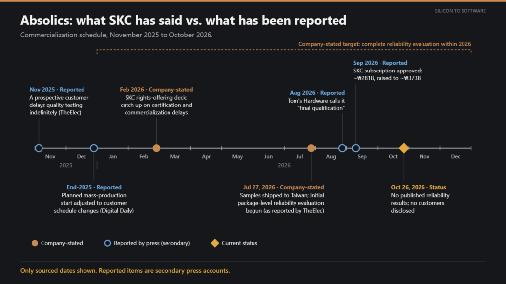
A month earlier, on its July 27 earnings call, SKC described where the program stood. As reported by TheElec, SKC said it had shipped embedded glass-core samples from its Covington, Georgia plant to Taiwan and begun an initial package-level reliability evaluation. TheElec framed that evaluation as the last technical verification before mass production.
Both descriptions point at the same stage. The difference is position within it. Absolics had entered what may be the final evaluation stage; it had not completed qualification. The distance between entering that stage and clearing it is where glass substrates for AI chips sit in 2026.
Engineering demonstrations exist. Customer qualification, repeatable production yield, and manufacturing economics have not been established publicly by any supplier. The schedule slips are not uniform. Absolics’ delay is documented in its parent company’s own financing materials. No revised Intel timeline was identified in the sources reviewed for this article.
This article covers three things:
- Why AI packages are straining organic cores.
- What glass measurably improves, and what depends on the design.
- Where Absolics, Samsung Electro-Mechanics, and Intel each stand, and what still separates a qualified substrate from a manufacturable one.
Two decades in PCB manufacturing and technical sales have taught me to recognize this stretch of a technology’s life: new-product-introduction (NPI) builds, qualification lots, customer sign-off. It is where new substrate technologies either earn a place in production or stall.
Why AI packages are outgrowing organic substrate cores
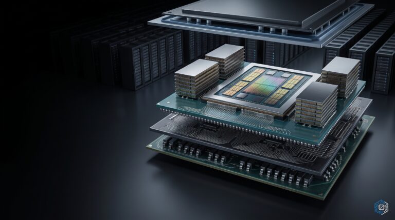
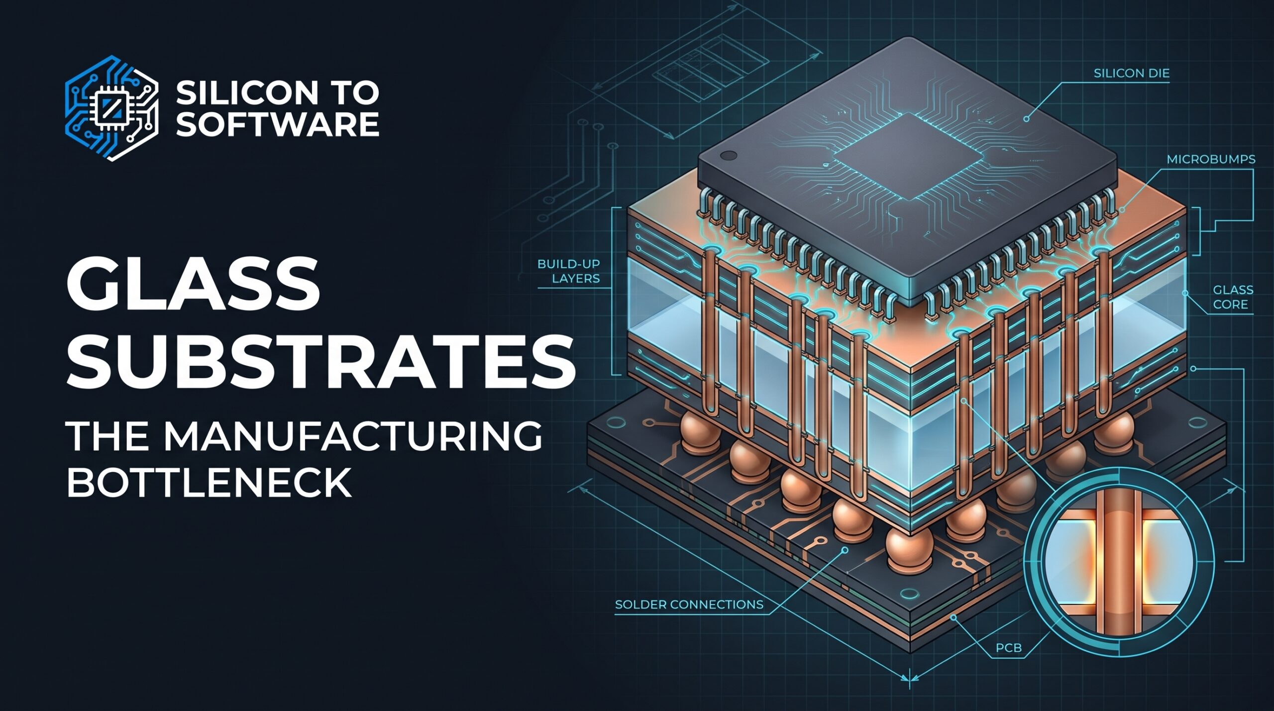
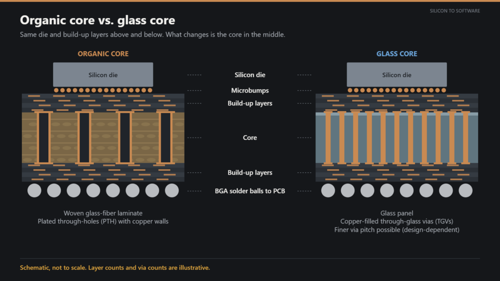
Today’s high-end package substrates use an organic core: a woven glass-fiber laminate, close cousin to a PCB core, with build-up layers on both sides. That construction has scaled for decades. Large multi-die AI packages are pushing it hard.
The mechanism is coefficient-of-thermal-expansion (CTE) mismatch. A package stacks materials that expand at different rates: silicon die, core, build-up dielectric, copper, solder resist. Every thermal excursion in fabrication and assembly bends the stack. Amkor’s warpage analysis notes that substrate suppliers have been moving toward larger and thicker cores to mitigate warpage as body sizes grow.
Intel’s demonstrations show the scale being targeted. According to TrendForce’s report of Intel’s NEPCON Japan 2026 showing, Intel’s EMIB (Embedded Multi-die Interconnect Bridge)–in-glass engineering sample is a 78 × 77 mm package supporting about 1,716 mm² of silicon, roughly twice the reticle limit. At that size, warpage becomes a primary constraint on assembly yield, coplanarity, and layer-to-layer registration.
Organic substrates are not standing still, though. Suppliers are adding core thickness and layer count to manage warpage, and Intel’s own 2023 materials stated that organic and glass substrates will co-exist. Glass is a candidate for the largest packages, not a guaranteed replacement.
I covered the organic-substrate side of this constraint, including ABF film supply, CoWoS capacity, and substrate qualification cycles, in The TSMC Arizona Bottleneck Isn’t the Wafer Fab: A $265B Warning for AI Chips. The CTE-mismatch and warpage mechanics behind multi-die packages are covered in Chiplets and Advanced Packaging: Why Substrate Capacity Is the Real Manufacturing Bottleneck.
What a glass core substrate fixes, and what depends on the design
Glass typically brings a higher elastic modulus than organic core materials, a CTE that can be tuned closer to silicon, and an extremely flat surface. How stiff and flat the finished substrate ends up still depends on its thickness and full layer stack. Those properties improve dimensional stability and lithographic alignment in the build-up layers.
Some of the most-quoted benefits are projections, not product measurements. When Intel announced its glass-substrate program in 2023, it described up to a tenfold increase in interconnect density and a 50% reduction in pattern distortion. Intel’s figures tie the density claim to vertical connections through the core: a through-glass via (TGV) pitch of about 100 µm, versus about 325 µm for organic plated through-holes, or roughly ten times as many vias per unit area. Those are company-stated figures, not measured product results. Electrical gains such as lower signal loss or better power delivery depend on the full package design.
The measured and modeled data is more useful, and more complicated.
Measured: warpage improved in OSAT test vehicles
According to SemiAnalysis’s ECTC 2026 conference review, Amkor and STATS ChipPAC, both outsourced assembly and test (OSAT) providers, measured 30–40% lower substrate-level warpage with a thinner glass core than their organic references. The same review notes assembly defects and TGV filling problems in that work.
The review reports the two companies’ results as a combined range. Per-company reference designs, stack-ups, and measurement temperatures aren’t given. The figure describes those test vehicles, not glass cores generally.
Measured: edge treatment decided survival in one study
The same review reports that STATS ChipPAC’s 74 × 74 mm glass-core packages failed across the test segments evaluated when no edge coating was applied; the review does not define those segments. Edge-coated versions completed assembly and reliability testing without abnormalities, and the coating reduced warpage by 33.5% compared with uncoated glass.
The review does not give sample counts, stress conditions, or failure criteria. This is one design’s result, not a general reliability benchmark.
Simulated: the board-level picture can reverse
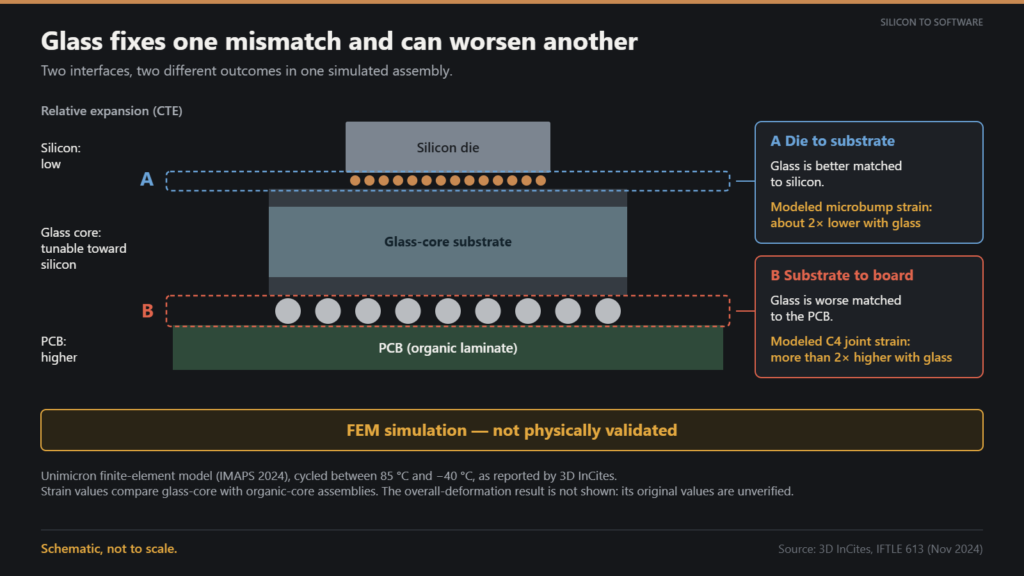
Unimicron presented finite-element modeling of a chip mounted on a glass-core substrate with microbumps, attached to a PCB with C4 bumps, cycled between 85 °C and −40 °C. As reported by 3D InCites from Unimicron’s IMAPS 2024 presentation:
- Overall assembly deformation: 3D InCites reported that Unimicron’s model showed greater deformation for the glass-core assembly. The original signed values and their interpretation remain unverified.
- Microbump inelastic strain: about 2× lower with glass. Glass is better matched to silicon.
- C4 solder-joint strain: more than 2× higher with glass. Glass is worse matched to the PCB.
These are simulation results, reported secondhand; the original paper was not available for this article. No physical validation of these values appeared in the sources reviewed. Higher modeled strain points to a potential solder-fatigue penalty, but the model does not establish joint lifetime or failure rates. The direction of the effect follows from the CTE mismatches involved, which is engineering inference, not test data.
Glass does not deliver a universal warpage reduction. It improves one mismatch, die to substrate, and can worsen another, substrate to board. Results depend on core thickness, glass composition, build-up materials, edge treatment, and test conditions. Different manufacturers’ designs will not behave identically.
Where Absolics, Samsung Electro-Mechanics, and Intel actually stand
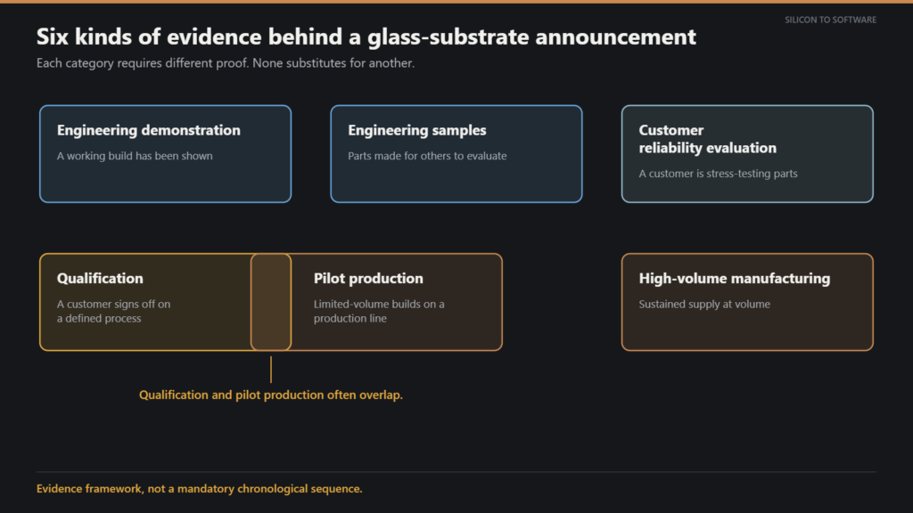
Every announcement can be classified by the evidence it provides:
- Engineering demonstration
- Engineering samples
- Customer reliability evaluation
- Qualification
- Pilot production
- High-volume manufacturing
This is an evidence framework, not a strict sequence. Customer qualification and pilot manufacturing often overlap. Each category requires different proof, and none substitutes for another.
| Program | Publicly evidenced stage | Schedule status | Key limitation |
|---|---|---|---|
| SKC / Absolics | Embedded: initial package-level reliability evaluation. Non-embedded: aimed at earlier commercialization | Delay acknowledged in SKC’s own capital-markets materials | No disclosed customers |
| Samsung Electro-Mechanics | Package-level verification with customer chips reported under way (Oct 2026). Glass core (GlaSSEM): 2H 2027 target. Finished substrates: full-scale operation from 2028 | Earlier 2027 finished-substrate baseline is secondary-reported only | Cause disputed; October progress is industry-sourced |
| Intel | Engineering demonstration and process development | No documented delay against its 2023 commitment | No disclosed customer qualification |
| TSMC / DNP | Panel-level and pilot-line programs | Glass in TSMC’s platform under review, per equipment supplier SCHMID; DNP targets FY2028 | Secondary sources |
SKC / Absolics: a delay the company has acknowledged
Absolics has a dedicated glass-substrate plant in Covington, supported by CHIPS for America awards: up to $75 million for the facility and a separate $100 million research award. Awards are not the same as disbursed funds.
Its commercialization schedule has also moved, and the company has said so in its own capital-markets materials. SBS Biz reported that the timeline has slipped by roughly three years. SKC’s February 2026 rights-offering presentation listed catching up on delays in certification and commercialization among the stated purposes of the raise. That is direct language for a capital-markets document.
Why it slipped has more than one reported explanation. These come from Korean press reporting and have not yet been checked against original filings for this article:
- Technical: Bloter reported that SKC’s offering filing cited a significant increase in technical variables in customer-specific mass production compared with original expectations.
- Customer timing: Digital Daily reported that a planned end-2025 mass-production start was adjusted to customer schedule changes.
- Demand: TheElec reported in November 2025 that one prospective customer had delayed its quality testing indefinitely, and that SKC considered large capacity expansion premature given near-term demand.
These factors can coexist; the public record does not rank them.
Absolics is pursuing two product tracks:
- Embedded: devices embedded in the glass core. This is the more difficult product, and it is in the initial package-level evaluation described above.
- Non-embedded: aimed at earlier commercialization. SKC’s February presentation pointed it toward RF and power-management applications.
SKC says it is working through reliability evaluation and certification with key customers, and plans to complete reliability evaluation within 2026. It has not disclosed which customers are evaluating its substrates. Names that circulate in industry reporting remain unconfirmed.
Samsung Electro-Mechanics: two deliverables, a disputed cause
Samsung Electro-Mechanics’ (SEMCO’s) timeline is easy to misread because two different products are involved:
- The glass core. GlaSSEM, SEMCO’s joint venture with Sumitomo Chemical’s Dongwoo Fine-Chem, will make the glass core. At signing on July 2, 2026, GlaSSEM planned to sample within the year and begin mass production from the second half of 2027. In a subsequent company response reported by TrendForce, SEMCO maintained that target of 2H 2027.
- The finished substrate. On its July 30 earnings call, SEMCO said it was building equipment and pursuing process stabilization and quality verification in stages, targeting full-scale operation of the glass-substrate business from 2028. The same company response reported by TrendForce distinguished the 2H 2027 glass-core material target from the 2028 finished-substrate target.
Some reporting compared those two dates and called the result a one-year delay. That compares different deliverables.
A narrower version is better supported. Newspim reported that SEMCO’s finished-substrate target had previously been 2027 and is now 2028, and that SEMCO attributes the timing to longer customer quality and reliability verification. That earlier 2027 baseline comes from secondary reporting. No primary SEMCO document stating it was located for this article.
The cause is disputed:
- Industry sources told TheElec that a prototype failed reliability qualification at a global communications chip customer.
- SEMCO has stated that no customer qualification has failed and that evaluation is ongoing.
Later reporting adds a stage marker. Citing industry sources, MoneyToday reported on October 6, 2026 that SEMCO had:
- completed reliability verification of the glass substrate itself after supplying customer samples
- moved to package-level verification with customer chips assembled on a 100 × 100 mm substrate
- set a target of starting its production line at the end of 2027
That is substrate-level progress, not completed customer qualification, and it is industry-sourced rather than a company disclosure.
Intel: an active glass substrate program without a verified delay
Intel’s record has been mischaracterized in both directions.
It has not abandoned glass. Rumors that it had were contradicted in January 2026, when Intel showed an EMIB-integrated thick-core glass substrate at NEPCON Japan. At ECTC 2026, according to SemiAnalysis’s review of Intel’s paper, Intel presented:
- a 510 × 515 mm glass-core panel with a 10-2-10 stack, described in the review as 24-layer (the layer-counting convention is unconfirmed)
- fully copper-filled TGVs
- two embedded EMIB bridges
- optical waveguides
Intel reports the panel was processed on existing organic-substrate lines. Singulated units showed no SeWaRe-type edge cracking (a lateral crack that starts at a diced glass edge, discussed below) after thermal-shock testing; the test conditions have not been independently confirmed.
It is not verifiably behind schedule. Its 2023 commitment was complete glass substrate solutions in the second half of this decade. That language describes when Intel expected to bring the technology to market; it does not name a product or a customer production date. Some reports discuss 2030-era timing for Intel’s glass substrates. Intel’s documented public commitment remains the second half of this decade, and no revised Intel date was identified in the sources reviewed for this article.
What Intel has not disclosed is a customer qualification or a production product. Its program sits at the engineering-demonstration and process-development stage.
TSMC and the wider field
TSMC’s panel-level packaging work should not be confused with a glass-core commitment. Equipment supplier SCHMID has described glass integration in that platform as under review rather than committed. Japan’s Dai Nippon Printing runs a TGV glass-core pilot line and targets fiscal 2028 for mass production. These are pilot-stage programs, not volume suppliers.
Where glass breaks: through-glass vias, interfaces, and edges
The schedules above all run through the same technical gate.
Glass can reduce one warpage problem while introducing a fracture-and-interface problem. Copper has a much higher CTE than glass. When a copper-filled TGV heats and cools, stress builds at the via wall, at the via caps, and along every copper/glass interface.
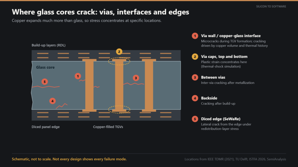
The research identifies where it fails:
- Copper volume and thermal history. A peer-reviewed IEEE study of conformally plated copper TGVs in fused silica, annealed at 400 °C, found no cracks below 12 µm of copper; at 12 µm and above, circumferential cracking increased exponentially.
- Fatigue at the via caps. TU Delft researchers thermal-shock-cycled copper-filled TGVs from −40 °C to 125 °C. Their simulations show plastic strain concentrating near the top and bottom caps, where copper meets glass.
- Defects across the process. An ISTFA 2026 study of glass-core substrates for AI server packaging identified three defect modes: microcracks during TGV processing, inter-via cracking after metallization, and backside cracking after build-up. The same study reported mitigations that passed its temperature-cycling and HAST testing. The abstract does not give sample sizes or acceptance criteria.
- Edge cracking. The industry term is SeWaRe: a lateral crack that starts at a diced glass edge under redistribution-layer stress. SemiAnalysis’s ECTC review called it the problem still unsolved.
The IEEE result is specific to its laboratory conditions:
- a 47.5 µm via, with copper on the walls rather than a fully filled via
- a glass with lower thermal expansion than typical glass-core materials
- a high anneal temperature
Production-oriented glass-core TGVs, such as those in Intel’s ECTC work, are fully copper-filled. The study shows that copper volume and thermal history drive cracking risk. It does not set a threshold for production glass cores.
Not every manufacturer encounters the same failure mechanisms; they depend on glass type, via geometry, metallization process, and build-up design. But the same categories recur across the studies cited here.
Why reliability qualification takes time
The PCB industry offers a relevant precedent, with an important limit.
In 2018 IPC published IPC-WP-023 on weak microvia interfaces. In a March 2019 industry warning, IPC noted that many microvia failures had occurred in products that had already passed traditional lot acceptance testing. The defect is a fracture at the interface between a microvia and the copper below it. It can be undetectable at room temperature and appear only when the board reaches reflow temperatures. IPC’s response emphasized performance-based testing that reproduces assembly reflow, using its existing IPC-TM-650 Method 2.6.27, which it was revising.
Glass-core IC substrates are not printed boards, and IPC Class 2 and Class 3 acceptance criteria do not govern them. The parallel is narrower: interface defects can be latent, invisible at incoming inspection, and revealed only by thermal stress. A demonstration alone can’t establish production-wide reliability. Qualification stress testing is designed to probe for it.
The same latent-failure pattern appears at board level, where assemblies that pass functional test can still fail after accumulating thermal cycles in service. See Industrial IoT Hardware Reliability: Why Boards That Pass Lab Testing Still Fail on the Factory Floor.
Package qualification typically draws on JEDEC stress methods:
- temperature cycling under JESD22-A104, which covers component and solder-interconnect testing
- humidity stress under JESD22-A110 (HAST)
For a new substrate material, it is reasonable to infer that customers layer their own requirements on top. Those criteria are rarely published, which is part of why qualification timelines look opaque from outside.
Depending on the failure, the fix can require new samples and another round of testing. SEMCO’s case illustrates the pattern without proving it. Industry sources said a new prototype would have to be produced and resubmitted, and that it couldn’t be done in a week or two. SEMCO disputes that any qualification failed.
Qualification is not production: process capability, yield, and economics
Passing qualification would be a major milestone. It would not prove that glass-core substrates are a viable manufacturing technology. Five distinct requirements are often blurred together. This is an analytical framework, not an industry standard:
- Reliability qualification. Evidence that parts built to a defined process survive the customer’s stress tests. It is the immediate technical gate.
- Process-window characterization. Mapping the range of process settings that produce good parts: copper thickness, cure profiles, edge treatment. Qualification samples are typically built inside a known window; production must stay inside it.
- Statistical process capability. Whether the process holds that window with margin, lot after lot, across tools and shifts. A process can produce qualifying parts without yet being capable in the statistical sense. Inspection is part of this: industry analysts note that a panel can carry more than a million vias, so catching an isolated killer defect requires high-speed in-line inspection.
- Sustained production yield. The fraction of panels and units that ship over time. No glass-core substrate maker has published production yield data that this article could locate.
- Commercial manufacturing economics. Competitive total cost against mature organic substrates, and the capital to build qualified capacity. That need not mean cost parity if glass enables larger or better-performing packages.
- Planned: SKC’s investment plan allocates Absolics funding across 2026, 2027, and 2028, covering capital and operating spending.
- Approved: in September 2026, SKC approved a subscription of about ₩281 billion in an Absolics rights offering, then raised its subscription to about ₩373 billion after Applied Materials did not take up its full allocation.
- Expansion: SKC has denied reports that Absolics’ second U.S. plant had been scrapped.
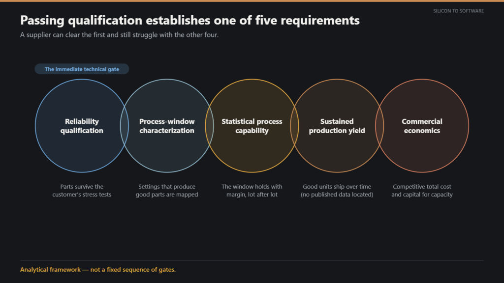
A supplier can clear the first and still struggle with the other four. That isn’t a case against glass. It’s a reason to read each announcement for which of the five it actually addresses.
What to watch next
Four observable milestones would signal whether glass-core substrates are moving from evaluation to commercial supply. They are independent indicators, not a required sequence:
- Absolics’ package-level reliability results. SKC has said it expects to complete reliability evaluation in 2026.
- GlaSSEM equipment orders. Whether SEMCO places them, signaling confidence in its production timeline.
- The first officially named glass-core customer at any supplier.
- TSMC’s decision on whether glass cores enter its panel-level packaging platform.
Glass’s material properties are good enough to get it into evaluation. Whether its copper/glass interfaces and edges survive qualification, and then hold up at production yield and cost, is still open.
A flat substrate is a materials result. A qualified substrate is a manufacturing result.
About the Author
Imran Valiani | Sales Director, PCB Electronics Manufacturing
20+ years working with major Bay Area and global tech clients. Founder of Silicon to Software, where I write about the hardware layer — PCB fab, AI gear, autonomous systems, and cyber — the stuff most tech writers have never touched. Literally.
Follow: X @SiToSoftware | LinkedIn
This article was developed with AI assistance and edited, fact-checked, and reviewed by the author. See my full AI disclosure.
Listen to the Silicon to Software podcast on Apple Podcasts, Spotify, or RSS.com — and watch on YouTube.
Sources
Sources are grouped by evidence type. Primary = the company, agency, standards body, patent office, or peer-reviewed record itself. Secondary = press or conference reporting about a primary event or document. Unresolved original = a publication the article relies on only through secondary reporting; the original was not accessed for this article.
A. Primary documents
SKC — “’26년 유상증자 설명자료” (2026 Rights Offering Presentation)
SKC, February 26, 2026
https://skc.kr/upload/ea/20260226/20260226175141765005.pdf
Supports: certification/commercialization delay catch-up as a use of funds; ₩589.6 billion glass-substrate allocation for 2026–2028; RF/PMIC two-track strategy.
Intel Newsroom — “Intel Unveils Industry-Leading Glass Substrates to Meet Demand for More Powerful Compute”
Intel, September 18, 2023
https://newsroom.intel.com/artificial-intelligence/intel-unveils-industry-leading-glass-substrates
Supports: second-half-of-decade roadmap commitment.
Intel — Glass Core Substrate briefing deck
Intel, September 2023 (third-party-hosted copy; not hosted by Intel)
https://www.igorslab.de/wp-content/uploads/2023/09/Glass-Core-Substrate.pdf
Supports: “Organic and glass substrates will co-exist.”
NIST CHIPS for America — Absolics (Covington, Georgia) facility award
National Institute of Standards and Technology
https://www.nist.gov/node/1853261
NIST CHIPS for America — Absolics advanced packaging research award (NAPMP)
National Institute of Standards and Technology (award date not independently confirmed for this article)
https://www.nist.gov/node/1867421
U.S. Patent 10,070,524 — “Method of Making Glass Core Substrate for Integrated Circuit Devices”
U.S. Patent and Trademark Office
https://image-ppubs.uspto.gov/dirsearch-public/print/downloadPdf/10070524
Supports: general background on glass-core stiffness relative to organic cores. Assignee not cited in the article.
Jung, H., Miller, D., and Jung, G. (Amkor Technology) — “Substrate Warpage Study for Heterogeneous Packages”
IMAPS, 2024
https://imapsource.org/article/129726.pdf
IEEE Transactions on Device and Materials Reliability — “Elimination of Thermo-Mechanically Driven Circumferential Crack Formation in Copper Through-Glass via Substrate”
Vol. 21, No. 3, pp. 354–360, September 2021 (IEEE article no. 9481891)
https://pure.uos.ac.kr/en/publications/elimination-of-thermo-mechanically-driven-circumferential-crack-f/
Institutional repository record. DOI and publisher URL not independently verified.
ASM International, ISTFA 2026 — “Comprehensive Failure Analysis and Mitigation of Glass Core Substrate Defects for Advanced AI Server Packaging”
ISTFA 2026 technical program, October 8, 2026
https://asm.confex.com/asm/istfa26/webprogram/Paper66092.html
Abstract only. Authors not confirmed for this article.
IPC — “IPC Issues Electronics Industry Warning on Printed Board Microvia Reliability for High Performance Products”
IPC, March 6, 2019
https://www.electronics.org/news-release/ipc-issues-electronics-industry-warning-printed-board-microvia-reliability-high
Supports: the 2019 warning, IPC-WP-023 (2018), and IPC-TM-650 Method 2.6.27. IPC-WP-023 and the method text were not separately accessed.
TU Delft Repository — glass through-via / glass-core record
Delft University of Technology
https://repository.tudelft.nl/record/uuid:f3f9fd11-e9e7-4c99-b44d-fab69bf0de27
Title and publication date not confirmed for this article.
B. Secondary reporting and conference reviews
SemiAnalysis — “EMIB-T, HBM4 Challenges, Microfluidic Cooling, Photonic Interconnects” (ECTC 2026 review)
SemiAnalysis, 2026
https://newsletter.semianalysis.com/p/ectc2026
Source for the Amkor/STATS ChipPAC warpage range, the STATS ChipPAC edge-coating result, Intel’s 510 × 515 mm panel, and the SeWaRe thermal-shock result.
3D InCites — “IFTLE 613: Solder Joint Reliability of Glass Core Substrate Assemblies”
3D InCites, November 2024
https://www.3dincites.com/2024/11/iftle-613-solder-joint-reliability-of-glass-core-substrate-assemblies/
Source for the Unimicron simulation results.
Luke James, Tom’s Hardware — “Glass substrate roadmaps examined — Absolics in final qualification and a first product that keeps slipping”
Tom’s Hardware, August 27, 2026
https://www.tomshardware.com/tech-industry/manufacturing/glass-substrate-roadmap-examined
TrendForce — “[News] Intel Reportedly Presents First Thick-Core Glass Substrate with EMIB, Targeting AI Data Centers”
TrendForce, January 26, 2026
https://www.trendforce.com/news/2026/01/26/news-intel-reportedly-presents-first-thick-core-glass-substrate-with-emib-targeting-ai-data-centers/
Source for Intel’s 78 × 77 mm package and ~1,716 mm² silicon area (Intel primary not located).
remio — “Intel Picks Lens Technology for a Glass Packaging Test, but Production Is Not Guaranteed”
remio
https://www.remio.ai/post/intel-picks-lens-technology-for-a-glass-packaging-test-but-production-is-not-gua
Source for the 100 µm vs. 325 µm via-pitch comparison (Intel primary brief not located).
TheElec — “앱솔릭스, 대만서 임베딩 유리기판 패키지 레벨 평가 돌입…’굿 다이’ 제작 성공”
TheElec (Korea), July 2026
https://www.thelec.kr/news/articleView.html?idxno=60117
Report of SKC’s Q2 2026 earnings call. Call transcript not accessed.
TheElec — “Absolics close to getting AMD approval in glass substrate”
TheElec, November 4, 2025
https://www.thelec.net/news/articleView.html?idxno=5476
SBS Biz — “SKC, 주가 뛰었지만 양산 안갯속…유리기판 플랜B 공식화”
SBS Biz
https://biz.sbs.co.kr/amp/article/20000313349
Bloter — “[단독] SKC, 美 유리기판 2공장 증설 ‘잠정 보류'”
Bloter
https://www.bloter.net/news/articleViewAmp.html?idxno=665814
Digital Daily — “SKC “앱솔릭스 美 글라스기판 2공장 백지화 사실 아냐””
Digital Daily, June 18, 2026
https://www.ddaily.co.kr/page/view/2026061814413292357
Dealsite — SKC / Absolics reliability-evaluation report
Dealsite, September 2026
https://dealsite.co.kr/articles/169146
Seoul Economic Daily — SKC investment in Absolics
Seoul Economic Daily, September 4, 2026
https://en.sedaily.com/finance/2026/09/04/skc-invests-200-million-in-absolics-to-speed-glass
CEO Score Daily — SKC Absolics rights-offering subscription
CEO Score Daily, September 23, 2026
https://ceoscoredaily.com/page/view/2026092313542645320
Asiatoday — SKC Absolics subscription increase
Asiatoday, September 28, 2026
https://www.asiatoday.co.kr/kn/view.php?key=20260928010009409
The ₩281 billion and ₩373 billion subscription figures rest on these three secondary reports (Seoul Economic Daily, CEO Score Daily, Asiatoday). SKC’s own releases on the subscription could not be retrieved, so these figures are not primary-verified.
Seoul Economic Daily (via Nate) — “삼성전기·스미토모화학, 유리기판 합작법인 ‘글라셈’ 설립…”2027년 양산 목표””
July 2, 2026
https://m.news.nate.com/view/20260702n29875
ETNews — “삼성전기 “AI·전장 고성장 시장 집중”…유리기판 2028년 양산 목표”
ETNews, July 30, 2026
https://www.etnews.com/20260730000332
TheElec — “Samsung Electro-Mechanics Delays Semiconductor Glass Substrate Investment”
TheElec, August 2026
https://www.thelec.net/news/articleView.html?idxno=12983
TrendForce — “[News] Glass Substrate War Heats Up: Shinko Electric Advances 22-Layer Product as Samsung Reportedly Faces Ramp-Up Uncertainty”
TrendForce, August 18, 2026
https://www.trendforce.com/news/2026/08/18/news-glass-substrate-war-heats-up-shinko-electric-advances-22-layer-product-as-samsung-reportedly-faces-ramp-up-uncertainty/
Sole located source for Samsung Electro-Mechanics’ August 19 statement (no customer qualification failed; evaluation ongoing; 2H 2027 glass-core material; 2028 finished substrates). Date anomaly: the page is dated August 18, 2026, yet reports a statement dated August 19, and it shows no update notice. A syndicated copy of the same August 18 article on LEDinside does not contain the company response, which suggests the statement was added to the TrendForce page after first publication; this is inferred, not confirmed. No independent source published on or after August 19 was located. Original company statement not accessed.
Newspim — “유리기판 2028년으로 밀린 삼성전기…FC-BGA는 풀가동·증설”
Newspim, September 7, 2026
https://www.newspim.com/news/view/20260907000377
MoneyToday — “반도체 기판 전쟁 다음은 유리…삼성전기, 내년말 생산라인 가동 목표”
MoneyToday, October 6, 2026
https://www.mt.co.kr/industry/2026/10/06/2026100615012220359
On Artificial Intelligence (IDTechEx coverage) — glass interposers and substrates in advanced packaging
https://www.onartificialintelligence.com/articles/33856/glass-interposers-and-substrates-in-advanced-packaging
JEDEC JESD22-A104, Temperature Cycling — standard listing
GlobalSpec standards index
https://standards.globalspec.com/std/14340837/jedec-jesd-22-a104
Index listing; standard text not accessed.
JEDEC JESD22-A110, Highly Accelerated Temperature and Humidity Stress Test (HAST) — summary
eesemi.com
https://eesemi.com/jedec.htm
Secondary summary; standard text not accessed.
C. Unresolved original publications (cited via secondary reporting only)
These originals were not accessed. Every claim drawn from them is attributed in the article to the secondary source listed in Section B.
- Intel — “Glass Core Substrates – Next Generation Advanced Packaging Platform for AI and HPC”, IEEE ECTC 2026. Reported via SemiAnalysis. The “24-layer” (10-2-10) layer-count convention is unconfirmed.
- Amkor Technology — “Evaluating Large Body Packaging Performance of Glass Core Substrates for AI and HPC Applications”, IEEE ECTC 2026. Reported via SemiAnalysis.
- STATS ChipPAC — “Assembly and Reliability Characterization of Glass-Cored Substrate Package for AI/HPC Applications”, IEEE ECTC 2026. Reported via SemiAnalysis.
- Unimicron — solder-joint reliability simulation of glass-core substrate assemblies, IMAPS 2024. Reported via 3D InCites. Exact title, authors, and signed deformation values unverified.
- SKC — Q2 2026 earnings call. Reported via TheElec. Transcript not accessed.
- Samsung Electro-Mechanics — August 19, 2026 statement. Reported only via TrendForce (page dated August 18, 2026; see the date note in Section B). Original statement not accessed, and no other report of it on or after August 19 was located. Newspim (September 7, 2026) separately reports the company attributing the schedule change to prolonged customer evaluation, but does not reference the August 19 statement.