Chiplets and Advanced Packaging: Why Substrate Capacity Is the Real Manufacturing Bottleneck
A hardware-industry look at the CTE mismatch, yield economics, and capacity constraints that decide whether a next-generation chip package actually ships.
Table of Contents
Chiplets and advanced packaging are the semiconductor industry’s answer to a scaling problem lithography can no longer solve on its own — and the reason that answer actually works starts with a number most engineers have never had reason to think about.
Silicon expands at roughly 2.6 to 3 parts per million per degree Celsius. The organic substrate underneath it in a modern IC package — ABF or BT resin, depending on grade and construction — expands somewhere in the range of 13 to 17 ppm/°C. Read off a materials table; that gap looks like a footnote.
At package scale, it’s a coupled thermomechanical problem — stack construction, panel dimensions, temperature excursion, and assembly process all feed into it — and it shows up as warpage, cracked microbumps, and a package that fails reliability testing after the electrical design has already been signed off.
(The same “don’t trust the headline datasheet number” lesson applies one level up the stack, too — see our comparison of Megtron 6, Megtron 8, and Tachyon 100G laminates for AI hardware, where construction and copper grade move the real numbers as much as the resin choice does.)
That’s the engineering reality behind one of the biggest architectural shifts in high-performance semiconductors in the past decade: the accelerating move toward chiplets and advanced packaging in AI accelerators, server processors, and other large, complex designs. This isn’t a universal industry shift — MCUs, analog, power, and cost-sensitive consumer parts remain overwhelmingly monolithic because advanced packaging would be economically irrational there.
But for the segment where it applies, most coverage of this shift focuses on the silicon — who’s building which chiplet, whose interconnect scheme is faster. What gets far less attention is what actually determines whether any of it can be manufactured at volume: substrate capacity, registration tolerance, and multiplicative yield economics.
This article breaks down what’s actually happening on the packaging floor — the difference between 2.5D and 3D integration, why substrate and interposer capacity has become the binding constraint on AI hardware roadmaps, why “chiplets are cheaper” is only conditionally true, and what engineers should be doing differently at the floorplan stage to avoid finding this out the expensive way.
Why Monolithic Scaling Stopped Making Sense
For 60 years, the industry’s default answer to “how do we get more performance” was to shrink the transistor and pack more of them onto a single die. That approach ran into a ceiling from two directions.
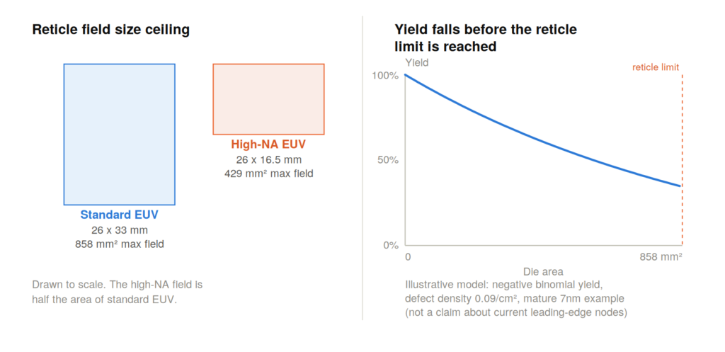
The physical ceiling: reticle limits. Lithography imposes a hard cap on maximum single-exposure die size. Standard EUV and immersion lithography tools have a maximum field size of 858 mm² (26mm by 33mm). High-NA EUV’s anamorphic optics halve the field in one dimension, producing a single-exposure field of roughly 26mm by 16.5mm — about 429 mm².
That’s a single-exposure field limit, not an absolute cap on functional die size — designs larger than the field can use reticle stitching across multiple exposures, a technique the industry is already actively developing for exactly this reason. Stitching isn’t free, though: it adds overlay, mask, productivity, and yield challenges of its own, which is part of why chiplet partitioning is often the more practical answer for designs that would otherwise need to stitch.
The economic ceiling: yield. Long before a design hits the reticle wall, yield economics usually make it uneconomical first. Using a negative binomial yield model — a widely used framework for this kind of estimate, though not the only one — with a defect density around 0.09 defects/cm² reported for a mature 7nm process (used here as an illustrative example of the mechanism, not as a claim about current leading-edge-node economics), yield falls off sharply as die area increases.
Past a certain die size, a monolithic chip stops being a rational thing to manufacture, regardless of what the process node can theoretically achieve. That’s the manufacturing-economics half of the story. The physics half is just as real: transistor features are now small enough that quantum tunneling — electrons passing through barriers that should stop them — is a hard physical limit, not just a yield problem. I go deeper on that atomic-scale constraint, and why it pushed the industry toward packaging in the first place, here.
A fair counterpoint. It’s reasonable to argue that packaging’s rise isn’t a competing bottleneck to lithography at all, but simply a downstream consequence of it — chiplets exist because monolithic scaling broke first, not because packaging independently became more important. That’s a legitimate reading of the causal chain.
This article’s practical claim is narrower than a causal one, though: regardless of which force gets credit for setting the shift in motion, the constraint that determines program schedule risk today sits in the package, not the transistor — and that’s the operating reality this piece is written for.
Chiplets are the industry’s response: split the design into smaller dice, connect them through advanced packaging, and let the package do the integration work the monolithic die used to do. That improves front-end die-yield economics — smaller dice are less exposed to defect density. It doesn’t eliminate yield risk; it moves part of that risk downstream, into die screening, bonding, and package assembly, which is exactly the trade-off explored later in this piece.
What gets skipped in most coverage is where the engineering difficulty actually went once the transistor stopped absorbing all of it. It moved from the fab to the packaging floor.
2.5D vs. 3D Integration: Two Manufacturing Problems, Not One
“Chiplets” and “advanced packaging” get treated as interchangeable terms in most coverage. They aren’t. 2.5D and 3D integration are distinct manufacturing approaches with different thermal, electrical, and yield profiles, and confusing them leads to bad assumptions at the design stage.
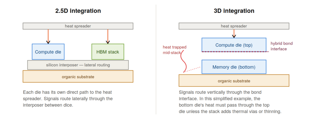
2.5D Integration
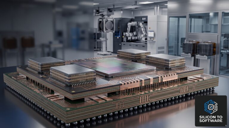
Multiple dice sit side by side on a silicon interposer, embedded bridge, or RDL interposer, connected through a redistribution layer (RDL) that routes signals laterally. TSMC’s CoWoS is one of the most prominent production examples of this approach, widely used in current AI accelerators where compute dice sit alongside HBM stacks on a shared interposer — but it’s one vendor’s implementation of the 2.5D category, not a synonym for it.
Intel’s EMIB (an embedded silicon bridge) and Samsung’s I-Cube (a silicon-interposer-based 2.5D architecture) are different approaches to the same 2.5D problem. Samsung’s X-Cube, by contrast, is a separate technology in that company’s portfolio for vertical 3D stacking — worth noting explicitly, since 2.5D and 3D branding across vendors doesn’t always map cleanly and is easy to conflate.
3D Integration
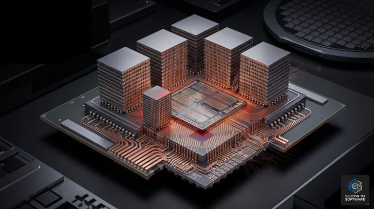
Dice stack vertically, with signals routed through through-silicon vias (TSVs) or, increasingly, direct copper-to-copper hybrid bonding with no bump material at all. The interconnect density gap between the two approaches is significant, not incremental: production copper microbumps have run around a 40µm pitch, with microbumps remaining viable down to roughly 10–20µm. Hybrid bonding is what takes over below that. AMD’s shipping 3D V-Cache, built on TSMC’s SoIC process, bonds at roughly a 9µm pad pitch in production today — genuinely sub-10µm, but not the sub-micron figures sometimes cited.
Those finer pitches are real on the research side: imec and EV Group demonstrated wafer-to-wafer hybrid bonding at a 200-nanometer pitch at ECTC 2026, with a production-relevant overlay accuracy on a full 300mm wafer. That’s a genuine R&D milestone, not yet the pitch running in a shipping commercial package.
Production and research capability are two different claims, and it’s worth being precise about which one a given number describes. There’s no bump material setting a mechanical floor on how tight the pitch can eventually go, which is why the roadmap keeps pointing finer.
Key Manufacturing Differences
| Factor | 2.5D | 3D |
|---|---|---|
| Interconnect path | Lateral, through interposer RDL | Vertical, through the die (TSV or hybrid bond) |
| Thermal path | Dice spread across a plane; more direct path to heat spreader | Higher thermal coupling; buried active layers can make hotspot removal harder unless the stack adds dedicated accommodations like thermal vias or backside thinning |
| Interconnect pitch | ~10–40µm (microbump-limited) | Sub-10µm achievable via hybrid bonding |
| Production yield maturity | Mature, high-volume | Newer at commercial volume; vendor-specific production yield figures (e.g., TSMC SoIC, Intel Foveros Direct) are not publicly disclosed |
Choosing between these isn’t a marketing decision. It’s a thermal and mechanical architecture decision, and RTL alone won’t catch the consequences of getting it wrong — that requires chip-package co-design, thermal and mechanical modeling, and electrical analysis addressed before hardware, not just after bring-up.
This is also where the package-level problem connects to a much bigger one: rising package-level power density is one of the root causes behind the rack-level AI cooling crisis data centers are now scrambling to solve with liquid cooling — the heat has to get out of the package before it ever becomes a facility’s problem.
The Real Bottleneck: Substrate and Interposer Capacity
Talk to people managing advanced packaging programs right now, and a consistent pattern emerges: the schedule risk isn’t wafer capacity. It’s downstream of it — split across two related but distinct constraints, and it’s worth being precise about which is which.
Constraint 1: TSMC’s own packaging-line throughput. CEO C.C. Wei told shareholders at the company’s June 2026 meeting that CoWoS advanced packaging capacity remained “extremely tight and sold out through 2026” — that’s a direct, on-the-record company statement.
The specific capacity trajectory is a separate matter: analyst estimates (not TSMC-disclosed figures) place it at roughly 35,000 wafers per month at the end of 2024, expanding toward a targeted 125,000 to 130,000 wafers per month by the end of 2026, though different analyst houses cite meaningfully different starting baselines for the same trend. Demand has continued to outpace the buildout either way. I go deeper on the CoWoS capacity numbers, the ABF substrate chokepoint underneath them, and TSMC’s $265B Arizona response in TSMC Arizona Bottleneck: A $265B Warning for AI Chips.
This data describes TSMC’s own packaging line specifically. It’s the most visible example of the constraint because TSMC is the most visible company in this space, not necessarily proof the same tightness applies equally at every OSAT and foundry running 2.5D or 3D packaging.
Constraint 2: upstream substrate material capacity. A related but separate constraint sits one step further upstream, at the substrate material itself, with a different set of suppliers. Ibiden, one of the largest IC substrate suppliers globally, announced in February 2026 a roughly ¥500 billion (about $3.18 billion) investment plan running through fiscal 2028, aimed at expanding high-performance IC substrate capacity for AI servers — that figure comes directly from Ibiden’s own announcement.
Unimicron raised its 2026 capital expenditure three times over the course of the year as demand kept outrunning its own guidance: from an initial NT$34 billion (~$1.1 billion) guided in February, to NT$53.7 billion (~$1.7 billion) by its July 2026 earnings call, with 80–85% of that spending concentrated in ABF substrate capacity.
Neither company runs TSMC’s packaging line — they supply the raw substrate material that packaging houses across the industry build on, TSMC included. That scale of investment from independent, competing suppliers is a meaningful signal that substrate capacity is tight industry-wide, not just at TSMC — but it’s a related constraint upstream of CoWoS capacity, not the same one, and treating them as a single bottleneck overstates how directly connected they are.
The Mechanism: Bump Pitch, Registration Tolerance, and Warpage
Interconnect density and package tolerance are linked, but not through a single number the way “bump pitch shrinks, therefore the substrate must match it” implies. Fine die-to-die pitch — the sub-40µm-down-to-sub-10µm range discussed above — is typically defined on a silicon interposer, embedded bridge, or RDL layer, which is a wafer-fab-style process with its own dimensional control.
The organic substrate underneath is a separate manufacturing domain: build-up layers, laser-drilled vias, line/space, and core construction, laminated at panel scale, with its own line/space and registration limits that don’t need to match interposer-level bump pitch directly. (This is a directional claim about the relationship between interconnect density and power efficiency, not a quantified one — vendors report GB/s-per-mm² and power-per-bit figures inconsistently across process generations, and no single comparable figure is cited here.)
What both domains share is the same underlying physics: the CTE mismatch between silicon and substrate material drives warpage, and warpage generally gets harder to control as package dimensions and thermal excursions increase — though the actual magnitude depends on the specific material stack, layer balance, die and interposer thickness, and assembly process, not on panel size alone.
This is the mechanism behind a pattern I’ve seen repeatedly on the DFM side: a registration or pitch capability demonstrated on a small test structure doesn’t automatically hold across a supplier’s full qualified production format. Dimensional stability, registration, and warpage have to be proven statistically at production panel scale, not inferred from a coupon — and that gap typically doesn’t surface until deep into qualification, the most expensive point in the program to discover it.
Why Chiplets Aren’t Automatically Cheaper
A common claim in mainstream coverage is that chiplets are simply cheaper than monolithic dies. The published cost modeling doesn’t support that as an unconditional statement.
Peer-reviewed cost frameworks for multi-chip integration — including a widely cited quantitative model known as “chiplet actuary,” published at the ACM/IEEE Design Automation Conference — model multi-chip integration as reducing total system cost primarily through yield improvement, package reuse, and the ability to mix process nodes across dice. That same research is explicit that the benefit is design-dependent: it’s largest for complex, high-transistor-count designs where a monolithic die’s area would otherwise suppress yield to uneconomic levels.
Industry cost analysis has described the failure mode directly: disaggregating a design can add cost through additional unique die designs, wafer-sort requirements, package components, assembly steps, die-to-die I/O overhead, and test insertions — and those added steps can offset the yield savings gained from smaller die area, particularly outside high-volume, high-complexity designs.
How much it adds depends heavily on the partition: a design built from several identical, replicated chiplets doesn’t need a unique mask set per chiplet, while a heterogeneous design mixing multiple process nodes and unique die types accumulates cost on every one of those axes.
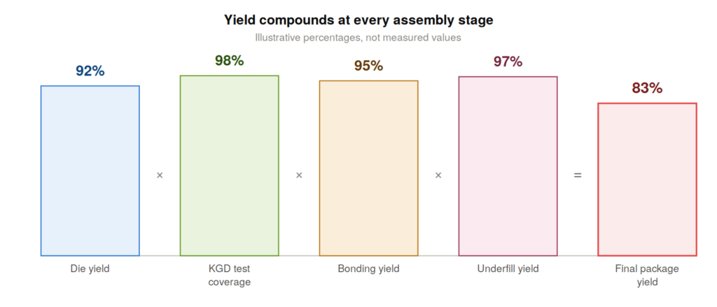
The underlying reason: Yield in a multi-die package is multiplicative, not additive. MicroLED displays hit the same math at an extreme: a native-RGB 4K panel carries roughly 25 million LEDs. Every die carries its own yield rate. Every bonding and assembly step adds its own yield loss. Multi-die integration raises the stakes on wafer-level screening and known-good-die strategy specifically because a defective die caught only after an expensive bonding step can destroy the value of an otherwise good package — a failure mode that doesn’t exist the same way in a monolithic part, where a bad die is scrapped before it consumes assembly cost on anything else.
That’s a real and meaningful cost driver even though monolithic parts already go through their own wafer probe, sort, and final test flow rather than a single end-of-line check.
Chiplets remain a sound strategy in the right conditions. The cost advantage is conditional on die size, defect density, production volume, and how much known-good-die testing burden the program can absorb. Framing it as an unconditional win skips the analysis that actually determines whether a given program is economically viable.
Who Actually Makes This Manufacturable
Public attention centers on the companies designing chiplets and the foundries fabricating them. Less visible: the OSATs (outsourced semiconductor assembly and test providers) and substrate suppliers who sit at different points in this chain and manage different failure modes. Substrate suppliers like Ibiden and Unimicron fight the registration-tolerance and CTE-mismatch battle at the panel-fabrication level, before a die ever touches the substrate.
OSATs like Amkor, ASE, and SPIL take over from there, managing die attach, bonding, and underfill at the assembly level, where a related but distinct set of warpage and alignment risks appears. Both are essential, and it’s the combination of both — against the multi-year capacity buildout timelines outlined above — that determines whether a design that looks manufacturable on paper actually ships.
Standardization is the other structural piece. Universal Chiplet Interconnect Express (UCIe) is the industry’s die-to-die interconnect standard, launched in March 2022 by a founding group that included Intel, AMD, Arm, Google Cloud, Meta, Microsoft, Qualcomm, Samsung, TSMC, and OSAT leader ASE, and formally incorporated that same year, in June 2022, with Alibaba and NVIDIA added as new board members.
The specification defines the physical layer, die-to-die protocol, and software stack, built on established PCIe and CXL standards — specifically enabling a design team to mix chiplets from different vendors rather than being locked into one company’s proprietary interconnect. (This describes UCIe’s 2022 founding and initial spec scope; it doesn’t track current adoption or the standard’s subsequent revisions.)
That matters practically: without a shared interconnect standard, a chiplet program has one more single-vendor dependency it can’t easily route around. UCIe doesn’t by itself make chiplets physically or electrically interchangeable — mechanical fit, power delivery, thermal envelope, firmware, and qualification still have to line up — but it removes one major barrier by standardizing the die-to-die communication layer itself.
Getting a large group of direct competitors to formally incorporate a standards body around that layer isn’t something this industry does casually, and the standard has kept moving since its 2022 founding: the consortium released UCIe 3.0 in August 2025, doubling peak link speed over the 2.0 spec and adding manageability features, while remaining backward compatible.
Scope note: This section covers manufacturability and supply-chain capacity specifically. It doesn’t address chiplet provenance or counterfeit risk in a multi-vendor supply chain, die-level test standardization, or the geographic concentration of advanced packaging capacity — heavily weighted toward Taiwan. Provenance and counterfeit risk specifically are covered in depth in our piece on counterfeit semiconductor chips; the geographic concentration question — including where, if anywhere, U.S. capacity is actually emerging across substrate, packaging, and PCB fabrication — is covered in Why US Chip Fabs Alone Won’t Fix the Electronics Supply Chain; die-level test standardization remains an open question for security and reliability engineers that warrants separate, dedicated coverage.
Designing for the Package: What Should Change in Your DFM Process
The practical takeaway for engineering teams: co-design the package from the start of a project, not after the floor plan is frozen. It’s the same underlying discipline problem covered in our piece on common PCB DFM mistakes — treating manufacturability as a final gate instead of an ongoing conversation with your fab and assembly partners — just showing up one level up the stack, at the package and substrate instead of the bare board.
A common and avoidable failure pattern: electrical engineers hand off a floorplan optimized purely for signal integrity and power delivery. The packaging and substrate team then flags bump pitch, escape routing density, or thermal via placement that the substrate supplier can’t actually hold in production. The result is a re-spin of a design that looked finished — because the interconnect scheme was never validated against what’s manufacturable at the registration tolerances the supplier can hold at panel scale, rather than what a lab demo achieved on a single coupon.
Practical steps to avoid this:
- Bring the packaging and substrate partner into the first floorplan review, not after tape-out.
- Validate target bump pitch against your specific supplier’s demonstrated panel-scale registration tolerance — not their best-case coupon data.
- Model warpage risk using your actual package size and material stack, not a generic reference design.
- Confirm known-good-die test coverage and cost early enough to factor into the yield/cost decision between chiplet and monolithic approaches.
Where This Leaves Engineering Teams
Transistor scaling still matters. Leading-edge nodes still carry real physical limits and real cost pressure — the reticle limit is real, and high-NA EUV is about to make it tighter, not looser. That pressure is exactly what pushed the industry toward chiplets in the first place.
But the constraint that decides whether a high-performance design actually ships on schedule has moved. It now sits in substrate registration tolerance, CTE-driven warpage, multiplicative yield across bonding steps, and whether an OSAT and substrate supplier — mid-way through a multi-billion-dollar capacity buildout — can hold a specification at volume that a lab demonstrated once.
The chip stopped being the product. The package is the product now. That’s the practical takeaway of chiplets and advanced packaging as an engineering discipline: teams that treat packaging as a first-order design constraint, on par with RTL, are the ones shipping on schedule and at a yield that makes the program worth running.
About the Data in This Article
Every specific figure in this article is sourced and dated in the sourcing notes accompanying this piece. Where public data doesn’t exist — such as vendor-specific production yield for hybrid bonding at TSMC or Intel — that gap is stated explicitly rather than estimated. One widely circulated claim (a specific chip product using glass-core substrates in early 2026) was excluded after a named semiconductor industry analyst publicly disputed it; conflicting sourcing on that point did not meet this publication’s standard for inclusion.
Why This Perspective
This analysis is written from a technical sales and DFM background inside the PCB and hardware manufacturing industry — the vantage point of someone who sits between engineering teams and the manufacturing floor, and who has watched packaging get treated as an afterthought in enough design reviews to recognize the pattern. That’s the frame for the recommendations in the DFM section above: they reflect what actually causes re-spins in practice, not a theoretical best-practices list.
About the Author
Imran Valiani | Sales Director, PCB Electronics Manufacturing
20+ years working with major Bay Area and global tech clients. Founder of Silicon to Software, where I write about the hardware layer — PCB fab, AI gear, autonomous systems, and cyber — the stuff most tech writers have never touched. Literally.
Follow: X @SiToSoftware | LinkedIn
For more analysis of chip scaling, advanced packaging, memory, and semiconductor engineering constraints, explore the Semiconductor Engineering & Advanced Packaging Resource Hub.
This article was developed with AI assistance and edited, fact-checked, and reviewed by the author. See my full AI disclosure.
Sources
- U.S. Patent 7,602,062 B2 — patents.google.com
- HilPCB: IC substrate and silicon CTE technical reference — hilpcb.com
- NextPCB: IC Substrate technical guide — nextpcb.com
- ASML: “5 things you should know about High-NA EUV lithography” — asml.com
- imec: “Imec demonstrates readiness of the High-NA EUV patterning ecosystem” — imec-int.com
- WikiChip: “Mask/Reticle” — wikichip.org
- SemiEngineering: “Are Larger Reticle Sizes On The Horizon?” and “Bumps Vs. Hybrid Bonding For Advanced Packaging” — semiengineering.com
- Chen, Li, Zhuang et al., “Floorplet: Performance-Aware Floorplan Framework for Chiplet Integration,” IEEE Transactions on Computer-Aided Design of Integrated Circuits and Systems, vol. 43, no. 6, pp. 1638–1649, June 2024, DOI 10.1109/TCAD.2023.3347302
- Feng & Ma, “Chiplet Actuary: A Quantitative Cost Model and Multi-Chiplet Architecture Exploration,” Proceedings of the 59th ACM/IEEE Design Automation Conference (DAC ’22), DOI 10.1145/3489517.3530428
- TechSearch International / DARPA presentation on 3D packaging interconnect roadmaps, December 2025
- Tom’s Hardware: reporting on AMD 3D V-Cache / TSMC SoIC bond pitch and TSMC CoWoS capacity commentary — tomshardware.com
- imec and EV Group: “W2W hybrid bonding with 200nm interconnect pitch” — imec-int.com
- TechTimes: TSMC CoWoS capacity coverage, citing TrendForce analysis — techtimes.com
- Ibiden Co., Ltd.: “Notice Regarding Capital Investment Plan for High-Performance IC Package Substrates,” February 3, 2026 — ibiden.com
- DIGITIMES: Unimicron 2026 capital expenditure guidance, February 2026
- Taiwan News: “Taiwan’s Unimicron targets record year on AI demand,” June 1, 2026 — taiwannews.com.tw
- BigGo Finance: coverage of Unimicron’s Q2 2026 earnings call, July 2026
- BusinessWire: “Leaders in Semiconductors, Packaging, IP Suppliers, Foundries, and Cloud Service Providers Join Forces to Standardize Chiplet Ecosystem,” March 2, 2022 — businesswire.com
- BusinessWire: “UCIe Consortium Announces Incorporation and New Board Members,” August 2, 2022 — businesswire.com
- UCIe Consortium: official specifications, including UCIe 3.0 — uciexpress.org
- Intel Foundry: Advanced Packaging (EMIB) technical documentation — intel.com
- Samsung Semiconductor: I-Cube and X-Cube packaging technologies — semiconductor.samsung.com
Note: vendor-specific production yield figures for TSMC SoIC and Intel Foveros Direct are not publicly disclosed and are not estimated in this article. Fast-moving capacity and capex figures (TSMC CoWoS wafer-per-month targets, Unimicron’s 2026 capex) reflect analyst estimates or the most recent company guidance available as of publication and may be superseded by later disclosures.