HBM4 Explained: Why Advanced Packaging, Not Bandwidth, Is the Real Constraint on AI Memory
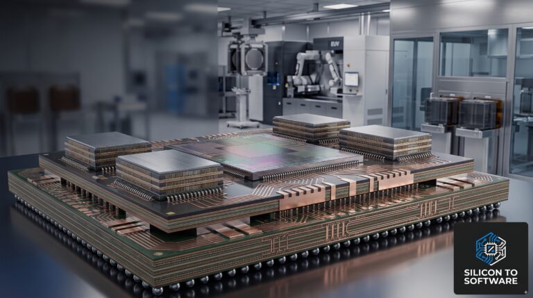
HBM4 delivers on its bandwidth promise — but the real HBM4 packaging bottleneck lies in interconnect density, thermal design, and power delivery, which now determine how many AI accelerators can actually be built.
Table of Contents
Earlier this year, according to reporting originating from two industry analyst firms — Global Semi Research and SemiAnalysis — widely syndicated but not independently corroborated by NVIDIA, TSMC, or any primary filing, NVIDIA’s original design for “Rubin Ultra” called for four compute dies and sixteen HBM4E memory stacks on a single package, built on TSMC’s CoWoS-L advanced packaging technology.
According to that reporting, the 2×2 die matrix produced severe substrate warpage under thermal and mechanical stress, and NVIDIA scaled the design back to two compute dies and eight HBM4E stacks roughly three months after unveiling it at GTC 2026, with TSMC’s longer-term panel-based packaging alternative, CoPoS, not expected at meaningful volume for several more years regardless. NVIDIA has not publicly confirmed this account.
The picture has since gotten more refined, not resolved. Three separate outlets — The Information, SemiAnalysis, and TrendForce — reported in early August 2026 on a related but distinct development: NVIDIA has been weighing a reduction in Rubin Ultra’s HBM capacity and stack height specifically, from an originally floated 12-Hi/288GB HBM4E configuration down toward options as low as 8-Hi/192GB.
That shift is driven by DRAM/HBM supply tightness expected through 2027, HBM4E validation and yield-ramp uncertainty, and rising memory costs — not by the substrate-warpage mechanism the earlier account described. TrendForce states plainly that “the final specification has yet to be determined.”
This isn’t necessarily a contradiction of the earlier warpage story so much as a different axis of the same unresolved picture. The original account concerned compute die count and total HBM stack count (four dies and sixteen stacks scaled back to two and eight); this more recent, better-corroborated reporting concerns the height and capacity of each individual stack, a separate design variable.
The two could describe sequential decisions rather than competing accounts of the same event — but either way, the through-line is the same: as of this writing, Rubin Ultra’s final memory configuration remains unsettled, on at least two independent axes, months after the platform’s original unveiling.
These two accounts may both be true — an early packaging setback followed by a later, separate supply-driven reconfiguration — or the more recent, better-corroborated TrendForce reporting may simply supersede the earlier warpage story. The honest position, as of this writing, is that Rubin Ultra’s final HBM configuration is unresolved, the mechanism behind any scale-back is contested between at least two different explanations (packaging yield versus memory supply), and no single account should be treated as the settled record.
That’s exactly why this article doesn’t rest its central argument on Rubin Ultra. It rests on JEDEC’s own published SPHBM4 standard, independent industry capacity estimates alongside TSMC CEO C.C. Wei’s own public statements on CoWoS allocation, and Samsung’s and SK Hynix’s disclosed manufacturing choices — independently sourced claims that don’t depend on any single vendor’s product roadmap turning out one way or another. Rubin Ultra, whichever account of it holds up, is illustrative of the pressure this article describes; it isn’t the evidence for it.
This article works through what HBM4 actually changed, why the industry’s own standards body is already offering an alternative path around part of the spec, and why the HBM4 packaging bottleneck — not DRAM bandwidth — is emerging as the real constraint on how many AI accelerators ship on schedule.
It’s also worth being precise about scope from the outset: this article moves across three distinct manufacturing domains that are related but not identical — HBM device manufacturing (DRAM yield, TSVs, die stacking), advanced package manufacturing (CoWoS, interposers, organic substrates, warpage, yield), and system-level PCB power and cooling (VRMs, vertical power delivery, board routing, cold plates). Treating pressure in one domain as automatically evidence of pressure in another is a mistake worth avoiding, and this article tries to keep the three separated rather than collapsing them into one undifferentiated “packaging problem.”
[Editorial note: six visuals have been produced for this piece — an HBM4 stack cross-section, a microbump/hybrid-bonding comparison, a CoWoS capacity-vs-demand chart, a thermal cross-section, a VRM placement comparison, and a vendor comparison table. Specific placement markers are inserted at the correct point in each section below.]
What HBM4 Changed at the Standard Level
HBM4 supports transfer speeds up to 8 Gb/s across a 2,048-bit interface for total bandwidth up to 2 TB/s, doubles independent channels per stack from 16 to 32, and was published by JEDEC as JESD270-4 in April 2025. It supports vendor-specific VDDQ levels of 0.7V, 0.75V, 0.8V, or 0.9V and VDDC levels of 1.0V or 1.05V, adds Directed Refresh Management (DRFM) for row-hammer mitigation, and maintains backward compatibility with HBM3 controllers.
That backward compatibility detail is easy to skip past, but it’s one real factor lowering the friction of adoption. A system integrator can adopt HBM4 without a new controller design cycle — the switching cost sits mostly in the package and interposer, not in the compute die’s memory interface logic.
The row-hammer detail is worth a moment too, because “RAS improvement” undersells what it addresses. Row hammer is a physical effect in DRAM: repeatedly activating one row (the “aggressor”) causes electrical charge leakage in physically adjacent rows (the “victims”), which can flip bits in data the aggressor row never touched.
It’s a side effect of cell density, not a software bug — it has to be mitigated in the memory itself, and prior approaches like Target Row Refresh have repeatedly been shown to be incomplete against newer attack patterns. DRFM is JEDEC’s row-hammer countermeasure for HBM4; the exact algorithmic distinction from TRR isn’t detailed in public JEDEC materials, so that specific improvement claim should be treated as unconfirmed rather than assumed.
That’s also where most technology coverage stops. The mechanism that makes the bandwidth gain possible — doubling the physical interconnect count — is what creates the packaging, thermal, and power delivery problems covered below.
Why the Interface Width Matters More Than the Bandwidth Number
Every one of HBM4’s 2,048 data signals needs a physical interconnect between the DRAM stack and the interposer or substrate beneath it — a silicon interposer and an organic substrate being different routing environments with different cost and signal-integrity profiles, a distinction that matters later in this piece. That interconnect has to fit at a pitch fine enough to pack that signal count into a die-sized footprint.
Worth noting: the 2,048 data signals are the headline figure, not the complete physical interface — the full interconnect count also includes command/address lines, clocks, power, ground, and control and test-related connections, meaning the actual pin-density pressure on the package is higher than the data-signal count alone suggests.
The HBM4 Packaging Bottleneck: Microbumps, Hybrid Bonding, and the SPHBM4 Workaround
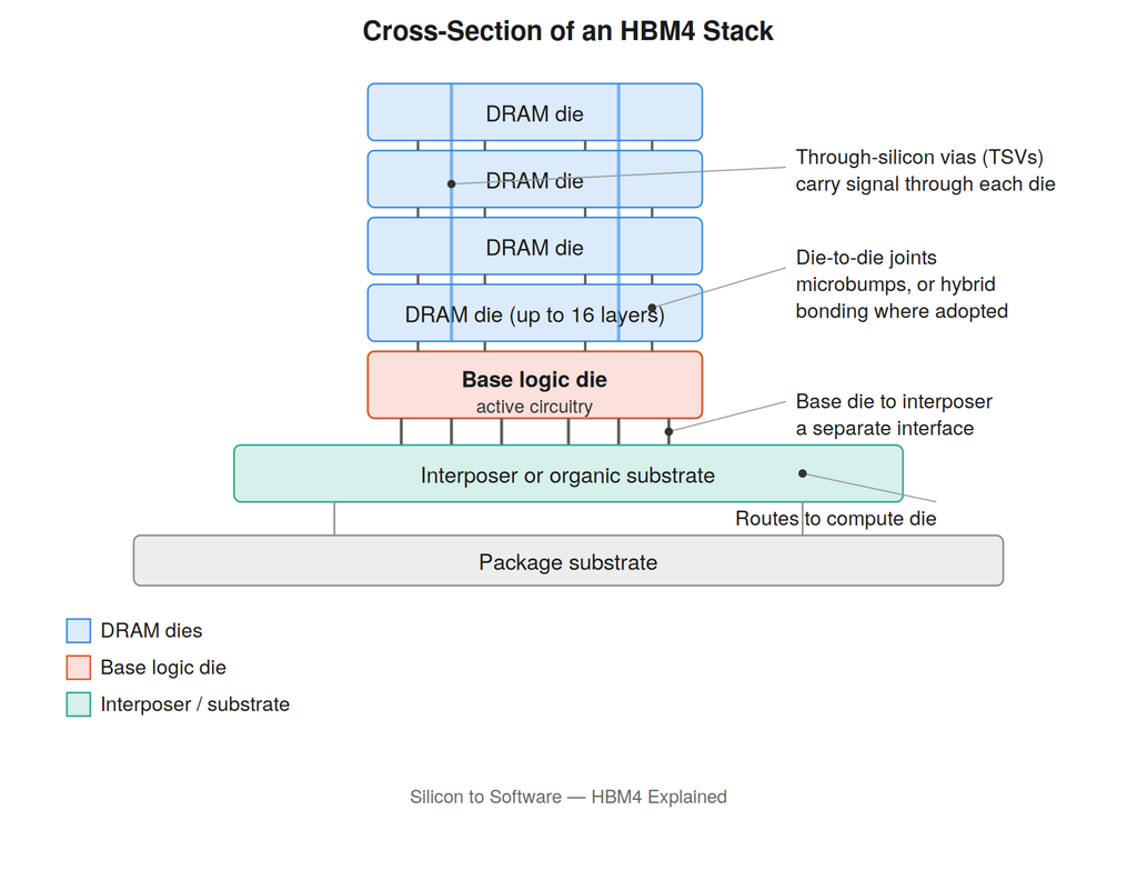
HBM4 was originally expected to require hybrid bonding — copper pads fused directly to copper, with a dielectric bond alongside the metal bond, eliminating microbumps and the standoff height they require. Multiple industry sources — including trade press coverage of the transition and analyst reporting on the packaging roadmap — describe HBM4 microbump pitch as moving from a historical range of roughly 40µm down toward approximately 10µm, and describe that same 10µm range as the point where hybrid bonding’s cost-per-connection starts to become competitive with microbumps.
That tracks with the broader industry pitch curve I’ve covered elsewhere — chiplet packaging generally sees microbumps remain viable down to roughly 10–20µm before hybrid bonding takes over, with AMD’s shipping 3D V-Cache already bonding at roughly 9µm in production. That 10µm figure is an industry-reported approximation for the microbump interconnect array specifically — it isn’t mandated anywhere in the JEDEC JESD270-4 electrical specification. Bump pitch is an OSAT/packaging-house implementation detail, and different sources use “pad pitch” somewhat loosely.
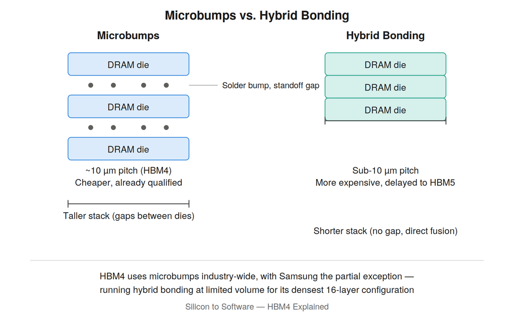
Two separate interconnect problems are worth keeping distinct here, because they’re easy to blur together. Inside the HBM stack, hybrid bonding — where adopted — replaces the microbump joints between individual DRAM dies (and between the bottom DRAM die and the base die), which is the interface most directly discussed above.
Separately, the base die still has to connect the assembled stack outward to the interposer or package substrate beneath it — a different physical interface that carries its own pitch and yield pressures and isn’t necessarily solved by whatever bonding method is used inside the stack. Both interfaces are under real pressure from HBM4’s wider bus, but they aren’t the same joint, and industry reporting doesn’t always cleanly separate them either.
It’s also worth being precise about what microbumps and hybrid bonding actually replace at the die level. Every die in an HBM stack is already connected vertically by TSVs — conductive channels drilled through the silicon that carry signals and power from one die to the next.
Microbumps and hybrid bonding are the two competing methods for joining the outside faces of adjacent dies together electrically; the TSVs are what carry the signal the rest of the way through each die. Hybrid bonding doesn’t replace TSVs — it changes how the die-to-die joint on top of them is made, which is why it can shrink stack height without changing the TSV architecture underneath.
Units built with hybrid bonding would struggle to compete on price against microbump parts, because microbumps — the cheaper, already-qualified process — set the market’s price floor. HBM5, expected toward the end of this decade, is now the generation where mass hybrid-bonding adoption is anticipated.
This is a trade-off that shows up constantly in high-reliability PCB and substrate manufacturing, just at a different scale: the technically superior process doesn’t win on introduction. The process that’s already de-risked in production, with known yield and known cost, wins — until the cost of not switching gets high enough to force the issue. This article doesn’t have a $/stack cost model to quantify that gap directly; the “uneconomical” framing here is qualitative, drawn from industry sourcing.
There’s a yield mechanic underneath this that rarely gets discussed outside packaging circles: once a stack is bonded, conventional die-level rework is essentially off the table. That’s exactly why manufacturers lean so heavily on known-good-die (KGD) screening and redundancy before stacking — testing each die in advance is the primary defense against ending up with an unreworkable, defective stack.
But screening isn’t perfect, and a defect that escapes it can compromise the value of the entire assembled stack rather than just one layer. That risk grows compounded as stack height increases, which is part of why the economics of switching interconnect processes are more sensitive than a per-bump cost comparison alone suggests.
Samsung’s Hybrid-Bonding Bet
Samsung is the partial exception, and it’s worth being precise about how partial. Its mainstream HBM4 mass production, like SK Hynix’s, primarily uses thermal-compression bonding with non-conductive film (TC-NCF), not hybrid bonding. Where Samsung differs is that it’s running hybrid copper bonding (HCB) in parallel at smaller volume — reported at roughly 10% of output — as an early-adoption path specifically for its 16-layer configuration, with broader commercialization targeted at the HBM4E stage rather than deployed as HBM4’s default today.
Samsung itself has claimed more than a 20% reduction in thermal resistance for HCB compared to traditional thermal-compression bonding — a company-stated figure from Samsung’s own GTC 2026 disclosures, not an independently measured result.
Samsung is wagering that pushing HCB into production early, even at limited volume, buys it a head start once wider hybrid-bonding adoption becomes necessary. Whether that wager pays off in yield and price at volume isn’t established in the public record yet.
JEDEC’s SPHBM4: Trading Interface Width for Easier Package Integration
The industry’s other response to interconnect density says something worth examining on its own terms. In July 2026, JEDEC published JESD330-4 — Standard Package High Bandwidth Memory (SPHBM4) — which uses the same DRAM dies as HBM4 but adds a new interface base die enabling mounting on standard organic substrates instead of silicon. SPHBM4 hits the same aggregate throughput as HBM4 with fewer pins by running at higher frequency: where HBM4 defines 2,048 data signals, SPHBM4 defines 512 with 4:1 serialization, specifically to relax the bump pitch needed for organic-substrate mounting.
JEDEC’s own materials describe the standard’s purpose in purely technical terms — enabling HBM4-class bandwidth on standard organic substrates rather than silicon interposers — and don’t frame it as a response to CoWoS-class packaging scarcity.
My interpretation, which goes beyond what JEDEC states directly: SPHBM4 is at minimum evidence that JEDEC sees real value in trading interface width for packaging flexibility, and commercially, that flexibility could also reduce dependence on scarce advanced-packaging capacity for companies that adopt it — though that specific commercial motivation is my inference, not a claim JEDEC makes. What SPHBM4 does not do is make HBM4 itself faster; it trades pin count for frequency to open a path to organic-substrate packaging for implementers who choose it.
The Geography Problem Behind “Packaging Capacity”
The number that determines how many HBM4-class parts exist in 2026 and 2027 isn’t the DRAM output figure. It’s advanced packaging throughput — and that throughput has a concentration problem worth stating plainly, one I’ve written about in more depth in a piece on the TSMC Arizona bottleneck, which covers the CoWoS-S/L/R capacity numbers and the IC substrate supply chain underneath them at length.
Industry estimates place TSMC’s share of leading-edge 2.5D advanced packaging capacity in the 90–95% range, overwhelmingly concentrated in Taiwan, though TSMC itself doesn’t publish an audited global market-share figure and the exact denominator varies by analyst. Some industry estimates put NVIDIA’s share of that capacity near 60%, with the top three customers together estimated above 85% — again, analyst tracking rather than disclosed allocation data.
TSMC’s own CEO has publicly acknowledged that CoWoS capacity remains extremely tight and sold out through 2026, and the company has begun outsourcing packaging steps to third parties like ASE and Amkor to relieve the pressure.
TSMC has broken ground on advanced packaging plants near its Arizona fabs, but as of this writing, chips packaged there still travel back to Taiwan for the process — the same gap between where a fab breaks ground and where the finished product actually gets built covered in Why US Chip Fabs Alone Won’t Fix the Electronics Supply Chain — meaning the geographic concentration risk isn’t resolved by the fabs’ physical location alone.
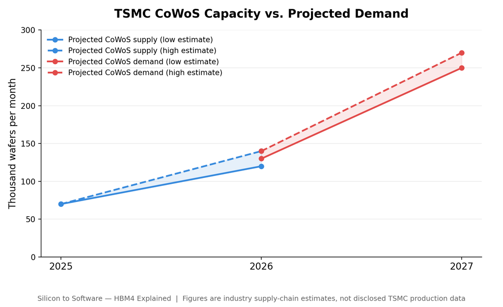
Capacity is genuinely growing — industry supply-chain estimates project TSMC’s monthly CoWoS output roughly doubling by the end of 2026 to somewhere in the 120,000–140,000 wafer range, up from a 2025 baseline that different analysts place anywhere from roughly 60,000 to 70,000 — but the same estimates project demand nearly doubling again on top of that, leaving a projected 10–20% shortfall even after the capacity build-out. These are forecasts, not disclosed TSMC production figures, and should be read as such.
TSMC is also working on a longer-term alternative: the company completed and began operating a pilot production line in August 2026 for its next-generation panel-based packaging technology, CoPoS, at its Chiayi facility, though the technology and its yields are expected to take roughly a year to stabilize even at pilot scale, and industry estimates still place broad volume production around 2028–2029.
This is the fuller picture: the HBM4 packaging bottleneck isn’t just a ceiling Rubin Ultra happened to hit. It’s a capacity race currently being run close on volume, concentrated almost entirely in one country, with one customer estimated to hold a large share of what exists — a scalability and supply-chain risk, not merely a packaging-engineering one.
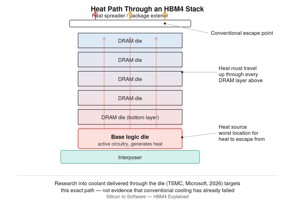
Thermal Design: Why the Base Die Is Now a Heat Source, Not Just an Interface Layer
Earlier HBM base dies were already doing more than nothing — they handled interface and control functions even in prior generations. What’s changed with HBM4 is a shift toward substantially more capable logic base dies, fabricated on logic rather than DRAM process nodes, with room for on-die power management, error-correcting code, and customer-specific accelerator logic — enabling “custom HBM” variants tailored to individual workloads.
That additional logic dissipates additional heat, and it’s positioned in a thermally challenging spot: buried beneath multiple DRAM layers, which increases the difficulty of extracting heat from active base-die circuitry compared to heat generated elsewhere in the package. AI accelerators have grown large enough, with fast enough interconnects, that the package itself is under real strain — circular interposers constrain package size and wafer utilization, HBM4E doubles I/O count while increasing speed, and multi-kilowatt packages are putting severe pressure on conventional cooling architectures.
This is the die-level version of a problem I’ve covered at the rack level too — by the time that heat reaches the data center floor, it’s the same crisis driving the shift to liquid cooling across the entire industry. At ECTC 2026, Samsung presented system-level thermal characterization of hybrid-bonded HBM on 2.5D advanced packaging, while TSMC and Microsoft demonstrated pushing coolant directly into silicon.
That last point is worth stating carefully: research into delivering coolant through or immediately adjacent to silicon demonstrates how aggressively thermal architectures may need to evolve as package power density keeps climbing — it doesn’t establish that today’s vapor chambers and cold plates have categorically stopped working. But it’s a strong signal of where the industry expects the ceiling to be.
Power Delivery: The Constraint Board-Level Engineers Should Watch Most Closely
Lower voltage reduces power per bit, which is why JEDEC specified VDDQ options down to 0.7V. It also compresses noise margin. A 2,048-bit interface switching simultaneously, on a 0.7V–0.9V rail, demands power delivery network (PDN) impedance control with very little room for error.
It’s important to lead with what this constraint is and isn’t, since it’s easy to blur the two. HBM4’s own VDDQ and VDDC rails draw far less current per stack than the compute die sitting next to them in the same package — none of the board-level power delivery figures that follow refer to HBM4 specifically. What the two problems genuinely share is competition for the same limited board and package real estate and design attention, which is a real constraint even though the current magnitudes on the two rails aren’t comparable.
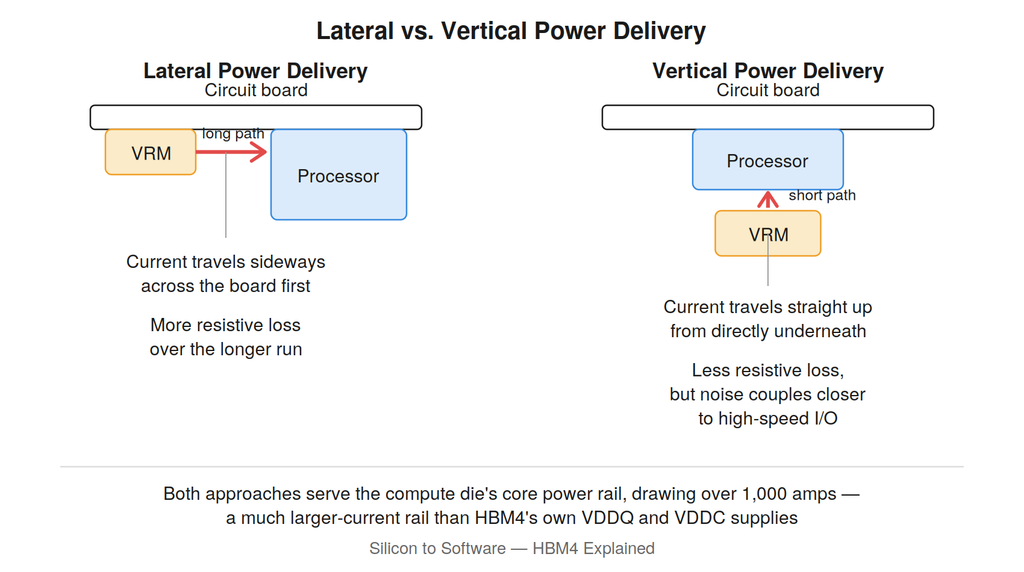
With that separation in place: a single AI GPU package now draws over 1,000 amps on its core compute power rail, and VRM placement has become a genuine trade-off: closer to the die reduces parasitic loss, but close enough to interfere, switching noise from the regulators couples into the high-bandwidth I/O linking accelerators together — a problem trade press coverage of power module design has flagged specifically on superchip designs like NVIDIA’s Grace Hopper, though this is analyst and industry-press reporting rather than an NVIDIA technical disclosure.
The industry’s response has been to move power delivery vertically, routing current up through the PCB directly beneath the processor instead of laterally across it; Empower Semiconductor’s Crescendo platform, for instance, is marketed by the company as supporting power domains of up to 3,000 amps through that path.
On current AI accelerator boards, multi-phase VRMs sit as close to the silicon as physically possible, and the PCB itself functions as a heat spreader under sustained current draw — a condition that stresses via barrels through Z-axis expansion and pushes laminate selection toward materials qualified for that thermal and mechanical load.
It’s worth being precise here: glass transition temperature (Tg) describes the point where a laminate’s resin shifts from rigid to rubbery, not a safe continuous operating temperature — a board should never run anywhere near its Tg in service.
High-Tg material is one relevant selection criterion for these boards, but decomposition temperature, Z-axis CTE, and resistance to conductive anodic filament growth all matter at least as much for reliability under sustained high current — the same kind of test-method and construction nuance I’ve broken down in more detail comparing Megtron 6, Megtron 8, and Tachyon 100G for AI hardware, where Tg alone is similarly a misleading number to compare across vendors without knowing the test method behind it.
On the HBM4-specific side of the problem: Intel and Samsung both presented ECTC 2026 papers addressing package-level PDN impedance for HBM4E — Intel’s EMIB-T embedded capacitors claiming an 82% improvement in PDN AC impedance, Samsung’s rebalanced interposer routing reducing impedance and voltage noise between the logic and HBM sides. EMIB-T is Intel’s own bridge-based packaging architecture, distinct from the CoWoS-L interposer approach implicated in the Rubin Ultra reporting above — this result demonstrates the general HBM4E PDN problem is being actively worked at the package level, not that CoWoS-L’s specific implementation has solved it.
No public source has yet characterized HBM4’s own power delivery network alongside compute-die vertical power delivery in a single shipping design. That gap — between package-level PDN work shown at a conference and board-level power delivery verified together in the field — is the actual constraint worth watching, and it’s narrower and more specific than “HBM4 has power problems too.”
Vendor Strategy: Two Different Bets on Where the Bottleneck Bites Hardest
The base-die logic node each vendor chose reflects a strategic split, not just a spec-sheet comparison.
- TSMC manufactures standard HBM4 base dies on its N12 logic node instead of a conventional DRAM process, cutting operating voltage from 1.1V to 0.8V for an expected ~1.5x efficiency gain — a company estimate reported via a single foundry presentation, not yet independently benchmarked; its custom C-HBM4E base die moves further to N3P, integrating memory controllers directly into the stack. SK Hynix runs this path through TSMC.
- Samsung states its HBM4, in mass production for the NVIDIA Vera Rubin platform since early 2026, delivers 11.7 Gbps per pin (up to 13 Gbps) on its sixth-generation 10nm-class (1c) DRAM process — a company specification, not an independently benchmarked shipping-system result. Samsung has since moved past the roadmap stage on HBM4E as well: in May 2026, it began shipping 12-layer HBM4E samples to major customers at a stated 14 Gbps sustained pin speed (scalable to 16 Gbps) and 3.6 TB/s per-stack bandwidth in a 48GB configuration — all company-stated figures describing sample-stage parts, not mass-production-qualified volume silicon. SK Hynix followed in June 2026 with its own HBM4E samples at up to 16 Gbps. As of this writing, HBM4E still has no unified JEDEC standard; each vendor’s numbers describe a different, non-interoperable implementation.
- Samsung’s SF4 logic base die costs more than SK Hynix’s TSMC N12 or Micron’s internal CMOS base-die technology, even with internal discounts. Samsung fabricates the logic die and handles 3D packaging under one roof — the only HBM4 supplier positioning itself as controlling the entire stack from silicon to final packaging, a framing that closely mirrors Samsung’s own marketing language.
[VISUAL PLACEMENT 6: vendor comparison table — insert here. Side-by-side spec table covering base-die node, bonding process, packaging model, pin speed, and Taiwan-concentration exposure for both strategies described above.]
One side is betting that alignment with TSMC’s packaging roadmap and lower-cost proven nodes wins the bottleneck. The other is betting that owning the entire stack, packaging included, wins it. SK Hynix’s TSMC dependency is direct and well documented through its base-die and CoWoS collaboration.
Samsung’s position is more genuinely independent: it markets integrated memory, foundry, and advanced-packaging capability under one roof, which gives it real manufacturing self-sufficiency for its own HBM stacks that SK Hynix doesn’t have. Whether that independence fully insulates Samsung’s supply chain from the broader Taiwan concentration problem — for instance, if its memory ultimately still gets integrated into GPU packages assembled on TSMC’s lines for major customers — isn’t something the public record clearly establishes either way.
If the Rubin Ultra reporting is accurate, it’s a data point against the TSMC-alliance side specifically, since it was reportedly TSMC’s packaging technology that hit the physical ceiling. It’s also a warning that no vendor’s packaging roadmap — Samsung’s included — has been stress-tested at that scale yet, at least not publicly.
What to watch next: if Samsung’s hybrid-bonded HBM4 ships at the volumes it’s promising for Vera Rubin, that’s evidence the vertical-integration bet is paying off faster than the packaging risk it carries. If NVIDIA’s scaled-back Rubin Ultra pushes incremental allocation toward SK Hynix’s TSMC-packaged stacks as a hedge against further CoWoS-L strain, that’s evidence running the other way.
The Bottom Line for Engineers Evaluating HBM4
HBM4 substantially raises the achievable memory bandwidth ceiling for AI accelerators, at genuinely improved bandwidth-per-watt, standardized and shipping on schedule. That’s worth stating plainly and without qualification — it’s a real engineering achievement.
It’s worth being precise about what that achievement does and doesn’t claim to solve, though. Even Samsung’s own public materials describe HBM4 as helping to “mitigate” data bottlenecks for AI computing, not eliminate them — appropriately narrower language than “fixed the bottleneck,” and worth matching here.
AI accelerator performance remains gated by plenty of factors beyond memory bandwidth alone: capacity, latency, compute utilization, interconnect and network bandwidth, and software efficiency all still bind independently. What this article has focused on is narrower and more specific: whether the packaging, thermal, and power-delivery ecosystem HBM4 depends on can keep pace with what the memory itself can now do.
On that narrower question: interconnect density is straining microbump economics industry-wide, with mass hybrid-bonding adoption pushed out to HBM5. Base-die logic is generating additional heat in a thermally difficult location. Package-level power delivery networks are being asked to hit a smaller target with less margin, inside a board-level power environment under its own separate pressure.
None of that is the constraint that should worry a systems architect most, though. The one that should is structural, not incidental: the advanced packaging capacity all of this depends on is concentrated overwhelmingly in one country, with estimates suggesting one company controls the large majority of it and one customer holds an outsized share of what exists.
That’s true independent of whether any single flagship design succeeds or stumbles in a given quarter — and Rubin Ultra’s own final configuration remains unresolved and contested between competing accounts, which is itself a reminder not to lean too hard on any one product story.
Two vendors are now running two different bets against that same structural fact — one leaning on TSMC’s roadmap and lower-cost proven nodes, the other betting that owning the entire stack, packaging included, buys enough independence to matter. Neither bet has been tested at scale yet, and neither fully escapes the concentration problem underneath it.
That’s the HBM4 packaging bottleneck worth tracking over the next several product cycles: not which vendor announces the next bandwidth milestone, but whether packaging capacity — geographically diversified or not — actually grows fast enough to keep up with what the memory itself can now do.
Related Reading
- TSMC Arizona Bottleneck: A $265B Warning for AI Chips
- Chiplets and Advanced Packaging: Why Substrate Capacity Is the Real Manufacturing Bottleneck
- AI Cooling Is the Next Bottleneck: Why Data Centers Can’t Keep Up With AI Hardware
- Why US Chip Fabs Alone Won’t Fix the Electronics Supply Chain
- Choosing the Right High-Speed Laminate for AI Hardware: Megtron 6 vs. Megtron 8 vs. Tachyon 100G
About the Author
Imran Valiani | Sales Director, PCB Electronics Manufacturing
20+ years working with major Bay Area and global tech clients. Founder of Silicon to Software, where I write about the hardware layer — PCB fab, AI gear, autonomous systems, and cyber — the stuff most tech writers have never touched. Literally.
Follow: X @SiToSoftware | LinkedIn
For more analysis of chip scaling, advanced packaging, memory, and semiconductor engineering constraints, explore the Semiconductor Engineering & Advanced Packaging Resource Hub.
This article was developed with AI assistance and edited, fact-checked, and reviewed by the author. See my full AI disclosure.
Sources
Standards
- JEDEC, “JEDEC and Industry Leaders Collaborate to Release JESD270-4 HBM4 Standard,” April 16, 2025 (jedec.org)
- JEDEC, “New JEDEC SPHBM4 Standard Enables HBM4-Class Bandwidth on Organic Substrates” (JESD330-4), July 13, 2026 (jedec.org)
Company disclosures
- Samsung Semiconductor Newsroom, “Samsung Ships Industry-First Commercial HBM4 With Ultimate Performance for AI Computing,” February 2026
- Samsung Global Newsroom, “Samsung Unveils HBM4E, Showcasing Comprehensive AI Solutions, NVIDIA Partnership and Vision at NVIDIA GTC 2026,” March 16, 2026
- Samsung Global Newsroom, “Samsung Electronics Begins Shipment of Industry-First HBM4E Samples,” May 29, 2026
- SK hynix Newsroom, “SK hynix Ships Samples of 12-Layer Next-Gen HBM4E,” June 18, 2026
- SK hynix Newsroom, “SK hynix Partners with TSMC to Strengthen HBM Technological Leadership”
- Empower Semiconductor, “Empower Debuts Revolutionary AI Power Delivery Platform to Solve Critical Technology Roadblock,” GlobeNewswire, October 2, 2024
Industry and analyst reporting
- TrendForce, “DRAM Supply to Remain Tight in 2027, Prompting NVIDIA to Lower HBM Configurations for Rubin Ultra,” August 4, 2026
- TrendForce, “Rubin Ultra HBM Specs in Flux as Supply Tightens,” research report, July 31, 2026
- TrendForce, “TSMC CoWoS Supply-Demand Gap Reportedly Seen Narrowing from 20% to 10% by End-2026,” June 15, 2026
- SemiEngineering, “HBM4 Sticks With Microbumps, Postponing Hybrid Bonding,” January 13, 2026
- SemiAnalysis newsletter, “EMIB-T, HBM4 Challenges, Microfluidic Cooling, Photonic Interconnects” (ECTC 2026 roundup), July 8, 2026
- SemiAnalysis newsletter, ISSCC 2026 roundup, June 18, 2026
- SemiHub, “HBM4 Bonding Technology — MR-MUF·TC-NCF·HCB Three-Track Split,” May 22, 2026
- EETimes, “The State of HBM4 Chronicled at CES 2026,” January 26, 2026
- Seoul Economic Daily, “TSMC Completes Line for Next-Gen CoPoS Packaging, Sees Year to Maturity,” August 11, 2026
- TechTimes, “AI Supply Crisis Moves Upstream: Advanced Packaging Becomes the Binding Constraint,” July 28, 2026
- Tom’s Hardware, “Hot Chips 2026: SK hynix pushes hybrid bonding to HBM5 as AI memory hits 775-micron ceiling,” August 2026
- TechPowerUp, TSMC N12/N3P C-HBM4E base-die coverage, December 1, 2025
- Nomad Semi (Moore Morris, Ray Wang), “Deep Dive on HBM,” June 3, 2025
Trade and technical press
- Electronic Design, “Inside Infineon’s Dual-Phase Power Modules for AI Power Delivery”
- Electronic Design, “Empower’s Voltage-Regulator IC Enables Vertical Power Delivery for AI Chips”
- Siemens EDA, “HBM3e and HBM4: IC Design Guide,” April 24, 2026
- NextPCB, AI accelerator PCB design guide
Note on sourcing standards: Company-stated performance figures (Samsung, SK hynix, Empower, Intel), analyst estimates (TSMC packaging capacity and market share), and single- or dual-sourced reporting (the Rubin Ultra configuration accounts) are labeled as such throughout the article rather than presented as independently verified fact. Several figures were cross-checked and revised during editorial review; where sources conflicted or a claim could not be independently confirmed, that uncertainty is noted in the text.