AI Chip Packaging Is the Critical Bottleneck of 2026
Google’s TPU, Amazon’s Trainium, and Microsoft’s Maia trade GPU flexibility for efficiency — but AI chip packaging capacity and power delivery, not chip design, decide how fast they scale.
Table of Contents
AI chip packaging, not chip design, is the constraint actually limiting how fast custom AI silicon can scale in 2026. Here’s the proof. On August 18, 2026, Marvell issued Google a warrant to purchase up to 58,970,907 shares of its stock — an aggregate exercise value of roughly $12.2 billion, disclosed the next day in a Marvell 8-K filing.
Most of that warrant doesn’t vest on a calendar. It vests in 240 tranches, one for every $500 million in custom chip revenue Google generates for Marvell through fiscal 2033. Marvell’s own filing describes this vesting as tied to discretionary purchases — Google’s future buying decisions, not a binding purchase commitment.
Read as a stock story, that’s a headline. Read as a manufacturing story, it’s a signal. A financial structure built around cumulative purchase volume, rather than a flat fee, suggests Google expects its custom-silicon buying to be large and sustained. That’s real signal about hyperscaler intent — though it’s worth being precise about what the filing does and doesn’t disclose, which this article gets into.
So what actually constrains custom AI silicon at scale? Five things: the real engineering trade-off between domain-specific accelerators and general-purpose GPUs, the advanced-packaging bottleneck that gates how fast any of these programs can scale, the power delivery engineering that competes with memory bandwidth for a shared design budget, the economic threshold that keeps hyperscale in-house silicon concentrated among a small number of firms, and the strongest argument against overreading this trend.
The Warrant Structure, Not the Number
Most coverage of the Google-Marvell deal focused on the $12.2 billion headline figure. The structure underneath it is more useful. And more limited than it first appears.
Of the total warrant, 1,360,867 shares vest in equal quarterly installments during the first year. The remainder vests in 240 equal tranches tied directly to purchase volume — one tranche per $500 million in Custom Products revenue Marvell books from Google, running from Marvell’s third fiscal quarter of 2027 through the end of fiscal 2033. The underlying agreement covers chips built around Google’s TPU ecosystem: AI inference accelerators, storage controllers, network interface controllers, memory interface controllers, and near-memory compute.
That word — discretionary — matters. This isn’t Google guaranteeing Marvell a fixed procurement volume. The filing discloses nothing about packaging-capacity reservations, CoWoS allocation, or queue priority. What it does is align Marvell’s equity upside with the scale of Google’s actual future purchases.
It’s reasonable to infer that this gives Marvell a stronger basis for planning capacity investment than a standard purchase order would. But that’s an inference about likely commercial effect, not a disclosed fact. Marvell itself is fabless. Whatever packaging capacity this deal ultimately depends on is capacity Marvell has to separately secure from TSMC and its OSAT partners, the same as any other customer.
Why Structure a Purchase Agreement This Way
Semiconductor capacity — wafer starts, advanced packaging slots, substrate supply — takes years to bring online. It doesn’t get built on spec. A supplier committing to expand that capacity needs demand certainty that extends past a single purchase order. Tying equity vesting to cumulative purchase volume gives Marvell a stronger signal to plan around than a standard supply contract would, while giving Google upside if the relationship scales as planned. Reasonable read of the incentive structure. Not a claim the filing itself makes.
What a Domain-Specific Accelerator Actually Trades Away
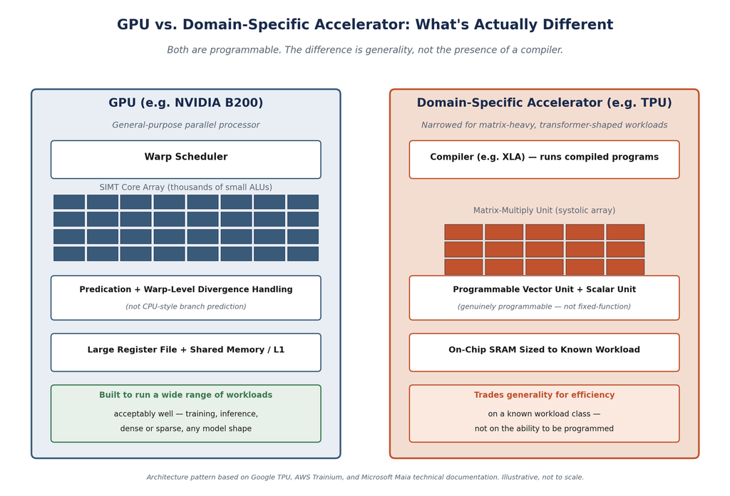
A GPU is a general-purpose parallel processor. It runs a mature software stack, handles training and inference, dense and sparse workloads, and absorbs next year’s model architecture largely through software.
So what’s actually different about a TPU? Not what most coverage assumes. A TPU, Trainium, or Maia is not a fixed-function device in the strict engineering sense — none of them are hardwired to a single operation the way a video codec block is. Google’s TPU contains a matrix-multiply unit alongside a genuinely programmable vector unit and scalar unit, and runs compiled programs through the XLA compiler.
AWS’s Trainium exposes tensor, vector, scalar, and general-purpose SIMD engines with a documented kernel-access interface. Microsoft’s Maia includes a programmable vector processor built on a custom instruction set. Domain-specific accelerators, both of them. Purpose-built and narrower than a GPU, but still programmable within their target domain.
What they trade away is generality, not programmability. That’s the whole distinction. Their compute units, memory hierarchy, and interconnect are architected around a known class of workload — matrix-heavy, transformer-shaped computation — rather than the broad range of parallel workloads a GPU is built to run acceptably well. That narrowing is where the performance-per-watt gain comes from: less silicon and power spent on flexibility the target workload doesn’t need.
The cost of that narrowing isn’t as automatic as it’s often made out to be. Software and compiler layers absorb a real share of workload change — a shift in attention mechanism or precision format doesn’t necessarily require new silicon if it fits within the accelerator’s existing architecture. What doesn’t get absorbed in software? A shift large and sustained enough to represent a genuinely different workload category.
At Google Cloud Next 2026, Google previewed an eighth-generation TPU architecture split for the first time into two separate chips — TPU 8t for training and TPU 8i for inference — after running both on a unified architecture for seven generations. Amazon made the same category-level split years earlier: Inferentia, for inference, launched in 2019; Trainium, for training, followed in 2020. That’s two distinct chips for two distinct workload categories by design, not a reactive one.
Google’s own announcement frames the 8t/8i split as intentional specialization for workloads that have diverged in their requirements, not as a correction to an architecture that failed. No public evidence this was an unplanned re-spin. What the split does show, reliably, is that hyperscalers plan dedicated silicon for known, distinct workload categories once volume justifies it — a real cost, paid in engineering effort and NRE, but a planned one.
The Strongest Case Against This Argument
The strongest pushback isn’t hardware. It’s software. NVIDIA’s advantage isn’t only performance-per-watt — it’s CUDA, and the tooling, libraries, and developer habit built on top of it over nearly two decades now (CUDA dates to 2006-2007, in case that number surprises you). This is hard to quantify with a clean number, and I won’t manufacture one.
But the direction is testable: a hyperscaler can buy its way into packaging capacity with enough capital and patience. It cannot buy a comparable shortcut through two decades of code and institutional familiarity built around a competitor’s platform. Not that easily. A domain-specific accelerator aimed at internal, well-characterized inference doesn’t touch that problem at all.
That’s visible even inside Google. Google Cloud sells both TPU and GPU instances to its own customers rather than steering everyone toward its own silicon. That’s evidence Google sees continued demand for both general-purpose GPU infrastructure and specialized TPU infrastructure — not proof that one is winning.
The spending data doesn’t support a clean substitution story either. Alphabet, Amazon, Microsoft, and Meta’s combined 2026 capital-expenditure guidance had climbed to roughly $730 billion by the time each company reported Q2 2026 results in late July — Alphabet raising its range to $195–205 billion, Amazon to about $220 billion, Meta to $130–145 billion, and Microsoft restating its calendar-year figure to roughly $175 billion (a shift the company attributed to a lease-accounting reclassification rather than a change in spending plans) — up sharply from the prior year and not all of it exclusively AI-labeled spend. That spending kept rising even as all four expanded custom silicon. Reads like a heterogeneous infrastructure buildout, not one category of chip quietly replacing another.
The Real Bottleneck: AI Chip Packaging Capacity
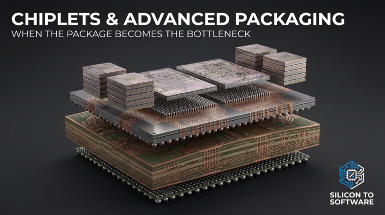
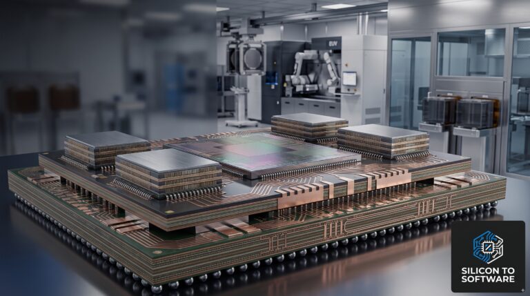
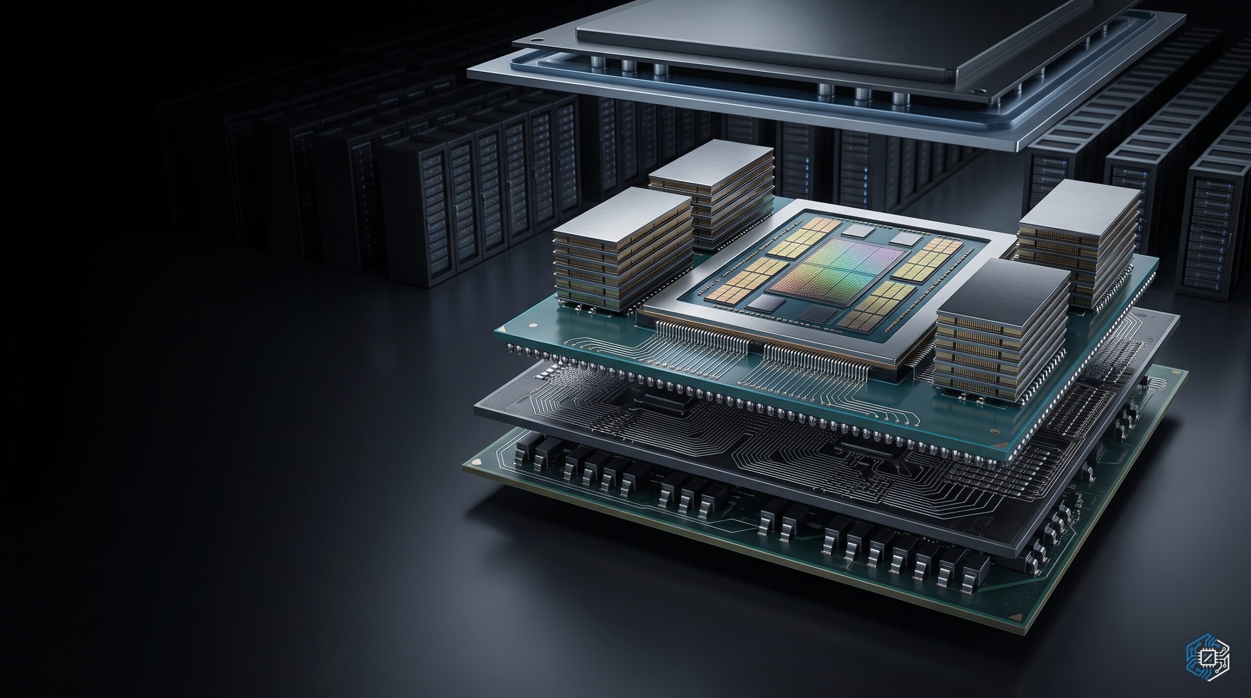
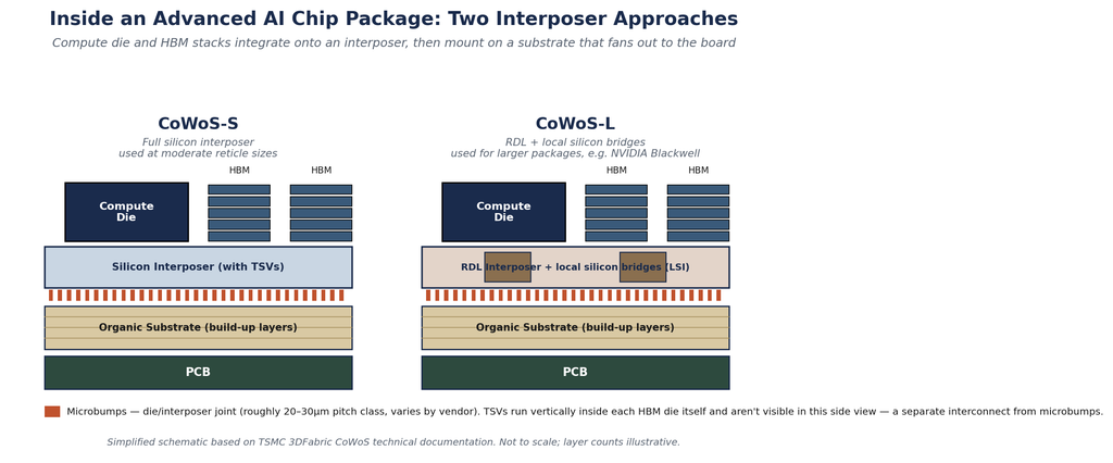
Coverage of custom AI silicon treats the chip as the product. Wrong frame. AI chip packaging is where the real story is: for the frontier data-center accelerators discussed here — Maia, B200, and the HBM-equipped TPU and Trainium generations — the chip is one component of a 2.5D or 3D package. Compute die and HBM stacks integrated onto an interposer, then mounted on a substrate that fans that density out to something a board can route to.
Interposer implementation varies by packaging generation: TSMC’s CoWoS-S uses a full silicon interposer with through-silicon vias; CoWoS-L, the variant used for NVIDIA’s Blackwell line, replaces that with an RDL-based interposer combined with embedded local silicon interconnect (LSI) bridges, per TSMC’s own CoWoS technical documentation — a design chosen specifically to scale past the size and yield limits of a monolithic silicon interposer.
(For a deeper look at the 2.5D-vs-3D distinction itself — bump pitch, CTE mismatch, and why multi-die yield is multiplicative rather than additive — see our breakdown of chiplets and advanced packaging.) Every layer of this stack is a manufacturing constraint:
- Interposer/RDL warpage. Larger packages carrying more die and HBM stacks are harder to hold flat through assembly thermal cycles. Warpage past tolerance produces bump-level opens or shorts at reflow.
- Stacking interconnects. HBM stacks connect DRAM dies vertically through through-silicon vias (TSVs) running through each die, then bond the completed stack to the interposer through microbumps — a physically separate interconnect from the TSVs. Microbump pitch varies by vendor and process rather than following one fixed industry number, but current HBM3E-class stacks are commonly reported in the roughly 20-to-30-micron range. HBM4 is expected to continue using microbumps at a tighter pitch — JEDEC raised the HBM4 stack-height limit specifically to accommodate this — with hybrid bonding (direct copper-to-copper bonding, eliminating microbumps) generally expected to phase in later, though the timeline diverges by memory vendor and some are reportedly moving earlier than others. Yield risk compounds with every added die and stack, since more interconnects mean more chances for one defect to affect the package.
- Substrate build-up layers. Fan-out from interposer to substrate to board runs through microvia structures with real aspect-ratio limits.
Yield Has Improved. Capacity Hasn’t Caught Up.
TSMC’s Vice President of Advanced Packaging Technology and Services stated at the 2026 OCP APAC Summit (August 11, 2026) that TSMC has reported CoWoS final-assembly yields consistently above 98% across multiple AI customer products, with some products reaching as high as 99%. That figure describes final package assembly yield on the configurations TSMC highlighted.
It doesn’t, on its own, establish a compound yield figure across every individual component (logic die, each HBM stack, interposer, substrate) that goes into a finished multi-die package, which is a distinct and generally tighter number in heterogeneous integration. Treat the 98–99% figure as a real, strong, company-stated data point about final assembly, not as evidence that yield is a solved problem end to end.
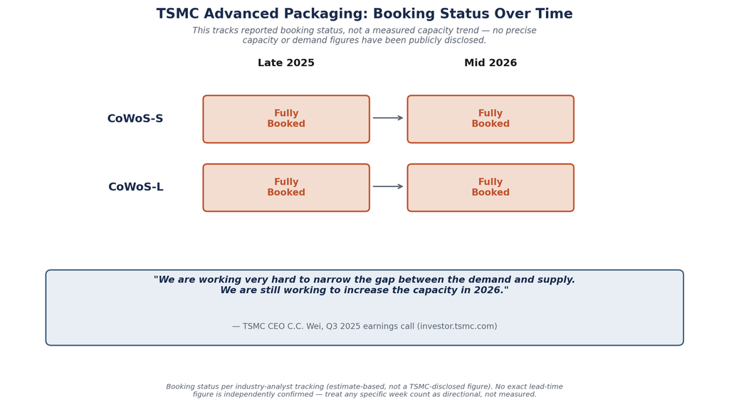
Capacity is the sharper constraint either way. As of late 2025, both of TSMC’s 2.5D packaging lines — CoWoS-S and CoWoS-L — were reported fully booked, with lead times estimated by industry trackers at roughly a year or more; that same estimate-based tracking still showed both lines fully booked as of a mid-2026 update, so this isn’t a stale snapshot — it’s a constraint that has persisted through the period this article covers.
No single named source confirms an exact week-by-week lead time, so treat the range as directional rather than precise. (For the specific monthly wafer-capacity trajectory and TSMC’s Arizona packaging buildout, see our TSMC Arizona bottleneck analysis.)
Trade press coverage of TSMC’s Q2 2026 earnings call, held July 16, 2026, reported that CEO C.C. Wei — responding to a question about competition from Intel’s EMIB advanced packaging technology — characterized CoWoS capacity as remaining extremely tight.
Google, Amazon, Microsoft, and NVIDIA all draw from the same constrained pool of packaging capacity at TSMC and its OSAT partners. A hyperscaler can finish the best domain-specific die design in the industry and still face a queue measured in months to build it. That’s the physical backdrop against which a deal structured around years of purchase volume, like Google’s warrant with Marvell, makes commercial sense — even though the filing itself is silent on packaging specifics.
Power Delivery — The Constraint That Competes With Memory Bandwidth
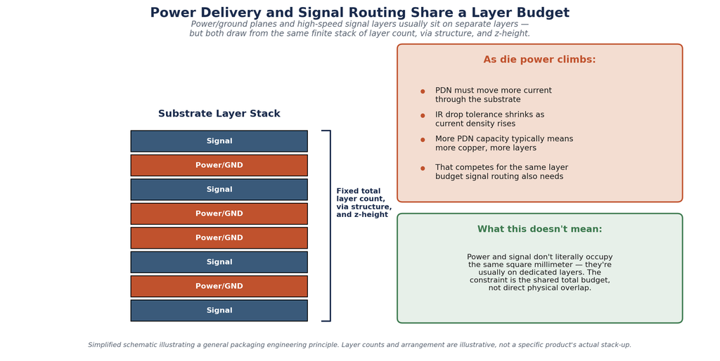
Package power is the second constraint. It competes with the first for a shared design budget rather than literal shared space. As die power climbs, the power delivery network (PDN) has to move more current through the substrate — and while power planes and high-speed signal layers are typically routed on dedicated layers rather than overlapping directly, they compete for the same finite budget of total layer count, via structure, and z-height.
Power delivery and high-speed signal routing may use different layers, but they still draw on the same finite package budget: copper layers, vias, routing space, and total z-height. More copper and shorter, lower-impedance power paths can improve current delivery, but those structures also consume space that must be balanced against signal routing, thermal paths, and mechanical constraints.
IR drop tolerance shrinks as current density rises, tightening PDN margin exactly where die power is going up.
What’s disclosed publicly here varies sharply by company.
| Chip | Disclosed power figure | Source type |
|---|---|---|
| Microsoft Maia 100 | 700W supported TDP, provisioned at 500W | Company technical presentation (Hot Chips 2024) |
| NVIDIA B200 (per-GPU) | 1,000W maximum (nvidia-smi reported), with a 700W default power limit configured in NVIDIA’s own DGX B200 system | Primary — NVIDIA DGX B200 User Guide (docs.nvidia.com) |
| NVIDIA DGX B200 (full platform) | 14.3 kW maximum system input, across six power supplies in 5+1 redundancy | Primary — NVIDIA DGX B200 User Guide (docs.nvidia.com) |
| Google TPU v7 (Ironwood) | No per-chip figure disclosed; Google states its 9,216-chip ICI network spans nearly 10MW at the pod level | Company presentation (Hot Chips 2025), pod-level only — do not divide by chip count |
| AWS Trainium2/3 | No official wattage disclosed for either chip; an AWS infrastructure VP has stated generally that chips above roughly 1,000W require liquid cooling, and that Trainium3 needs it while Trainium2 doesn’t | Executive statement, general threshold — not confirmed as a Trainium3-specific spec |
Worth being precise about the NVIDIA figure specifically: 700W is a configured power limit, not a measurement of what the GPU actually draws under typical workload — NVIDIA’s own documentation explicitly distinguishes a power-limit setpoint from an actual measured reading. The parallel to Microsoft’s Maia disclosure still holds structurally (a documented ceiling and a lower documented default limit), but neither figure describes real-time measured consumption.
The 14.3kW system figure also shouldn’t be divided by GPU count — it’s a platform rating across six redundant power supplies, not eight GPUs in isolation. (These same B200 power figures are also what’s driving the shift to liquid cooling at the rack level — see our look at why AI data center cooling is becoming the binding constraint for how that plays out once the chip leaves the package.)
Google and Amazon disclose less, and the reason isn’t as simple as “internal versus external.” Maia is actually the more instructive comparison here, not the exception it first looks like: Microsoft has not sold Maia as standalone hardware and, as of this writing, hasn’t even made it generally available as a cloud rental — it runs Microsoft’s own internal AI services and nothing else. That’s a more closed deployment model than TPU or Trainium, both of which are at least rentable through Google Cloud and AWS.
And yet Microsoft published detailed Maia power figures at a public technical conference. Google kept Ironwood’s chip-level wattage quiet. Amazon said even less about Trainium.
NVIDIA is the one clean case: it sells GPUs and systems directly to OEMs and enterprise customers who have to design infrastructure around the specs, so publishing numbers isn’t optional. For everyone else? Disclosure looks more like engineering-culture and conference-participation choices than a strict function of business model. Microsoft and Google have both used Hot Chips to put real numbers on the table despite neither selling hardware externally. Amazon and Google’s own TPU team have chosen not to, for Trainium and Ironwood specifically.
It’s worth being honest here: this article can describe the pattern more confidently than it can fully explain it.
Why This Kind of Custom Silicon Stays Concentrated Among a Few Firms
Custom silicon carries real non-recurring engineering (NRE) cost. Neither figure below is a foundry-disclosed price. Both are third-party analyst estimates. They also measure different things: mask set cost alone, versus the fuller design bill including EDA tooling, IP licensing, and verification.
Mask set costs alone have moved past $10 million at 7nm and are approaching $40 million at 3nm, per SemiAnalysis’s cost tracking — though other industry cost models put the 3nm mask-set figure closer to $10–20 million. Once EDA tooling, IP licensing, and verification are added on top of the mask sets, full chip design cost runs $400–600 million or more by some industry estimates.
Who This Math Actually Works For
| Hyperscaler (Google, Amazon, Microsoft) | Everyone else | |
|---|---|---|
| Internal workload volume | Large enough to amortize $400M+ NRE against known, category-level demand | Not enough volume to spread the cost |
| Capital position | Can eat a nine-figure design cost as a routine line item | A nine-figure design bet is a company-level risk |
| Packaging capacity access | Can commit years of purchase volume ahead — the Marvell warrant illustrates the mechanism | No comparable leverage to secure a queue slot early |
| Specialization exposure | Can absorb funding a second silicon program once a workload category justifies it (see TPU 8t/8i) | One design miss can sink the program |
Even at the low end of the NRE estimates, that cost only pencils out against enough volume to amortize it. Google, Amazon, and Microsoft can do that. Their internal inference workloads are large enough, at the category level, to justify it — even when, as the TPU 8t/8i split shows, that eventually means funding a second silicon program once a workload category grows large enough to warrant its own dedicated design.
This is the boundary worth stating directly: this isn’t a preview of every company eventually building its own AI chip. Far from it. Building hyperscale, leading-node, HBM-equipped accelerators in-house is a phenomenon specific to firms with internal demand at that scale and balance sheets that can absorb nine-figure design costs as a routine line item — a narrow set of companies, but not the only alternative to buying GPUs.
Merchant accelerator vendors, AMD’s GPU line, FPGA-based approaches, and startup-built ASICs all serve companies that don’t clear that threshold; the point isn’t that everyone else has no options; it’s that in-house hyperscale silicon specifically stays out of reach for most of them.
What to Watch Going Forward
The next stretch of this competition won’t be decided by benchmark tables alone. AI chip packaging and substrate capacity will be among the biggest factors determining who can actually ship at the volume their workloads demand — alongside power delivery, HBM supply, and how fast each company’s software stack matures.
The same pattern shows up in AI networking, not just compute. (See our breakdown of the co-packaged optics packaging bottleneck for how coupling-tolerance and laser-reliability constraints are quietly gating switch and interconnect deployment the same way CoWoS capacity gates accelerator deployment.)
That’s what the Marvell warrant’s vesting structure is actually worth paying attention to, once you read past the headline number. Not as proof of a guaranteed supply chain outcome — the filing doesn’t disclose that. As a real signal of how a hyperscaler expects its own purchasing to scale. For engineers and infrastructure planners evaluating this space, the more useful things to track are purchase-volume trends and packaging capacity announcements, not spec-sheet comparisons.
Author’s Note
This analysis draws on two decades in PCB manufacturing and hardware supply chain work — specifically, the DFM and advanced-packaging side of the industry where these design decisions actually get tested against yield, lead time, and cost. The die architecture comparisons in AI chip coverage are usually accurate as far as they go. What’s harder to get right from outside the industry? The packaging and power delivery layer underneath — the part that determines whether a design ships at volume, not just whether it works in a lab.
About the Author
Imran Valiani | Sales Director, PCB Electronics Manufacturing
20+ years working with major Bay Area and global tech clients. Founder of Silicon to Software, where I write about the hardware layer — PCB fab, AI gear, autonomous systems, and cyber — the stuff most tech writers have never touched. Literally.
Follow: X @SiToSoftware | LinkedIn
For more analysis of chip scaling, advanced packaging, memory, and semiconductor engineering constraints, explore the Semiconductor Engineering & Advanced Packaging Resource Hub.
This article was developed with AI assistance and edited, fact-checked, and reviewed by the author. See my full AI disclosure.
Sources
Primary / regulatory filings
- Marvell Technology, Form 8-K, filed August 19, 2026 — investor.marvell.com/sec-filings/all-sec-filings/content/0001193125-26-356217/d412696d8k.htm
- Marvell Technology, Warrant Exhibit 4.1 to the same 8-K — investor.marvell.com/sec-filings/all-sec-filings/content/0001193125-26-356217/d412696dex41.htm
Primary company technical documentation
- NVIDIA, DGX B200 User Guide — Introduction to NVIDIA DGX B200 Systems — docs.nvidia.com/dgx/dgxb200-user-guide/introduction-to-dgxb200.html
- NVIDIA, DGX B200 User Guide — Managing Power Capping — docs.nvidia.com/dgx/dgxb200-user-guide/power-capping.html
- Microsoft, “Inside Maia 100: Revolutionizing AI Workloads with Microsoft’s Custom AI Accelerator” — techcommunity.microsoft.com (Hot Chips 2024 disclosure)
- Google Cloud, “TPU 8t and TPU 8i technical deep dive” — cloud.google.com/blog/products/compute/tpu-8t-and-tpu-8i-technical-deep-dive
- Google Cloud, “AI infrastructure at Next ’26” — cloud.google.com/blog/products/compute/ai-infrastructure-at-next26
- Google, “Ironwood: The first Google TPU for the age of inference” — blog.google/innovation-and-ai/infrastructure-and-cloud/google-cloud/ironwood-tpu-age-of-inference
- TSMC, CoWoS technical overview (3DFabric) — 3dfabric.tsmc.com/english/dedicatedFoundry/technology/cowos.htm
- TSMC, Q2 2026 Earnings Call, July 16, 2026 (event reference) — investor.tsmc.com
2026 capital-expenditure guidance (Q2 2026 earnings, primary company sources)
- Alphabet, Q2 2026 earnings call, July 22, 2026 (CFO Anat Ashkenazi) — full-year 2026 capex guidance raised to $195–205B
- Amazon, Q2 2026 earnings call, July 30, 2026 (CEO Andy Jassy) — full-year 2026 capex guidance raised to ~$220B
- Meta Platforms, “Meta Reports Second Quarter 2026 Results,” July 29, 2026 — investor.atmeta.com — full-year 2026 capex guidance narrowed to $130–145B
- Microsoft, FY2026 Q4 earnings call, July 29, 2026 (CFO Amy Hood) — calendar-2026 capex expectation restated to ~$175B, reflecting a finance-to-operating lease reclassification, not a change in spending plans — microsoft.com/en-us/investor
Standards
- JEDEC, JESD270-4A:2025-11 (current HBM4 standard revision, superseding JESD270-4)
Industry / financial research and reporting
- SemiAnalysis — mask set and chip design cost estimates
- Financial Times, “Google outpaces rivals as Big Tech’s AI spending plans rise to $725bn” (May 2026) — earlier-quarter snapshot, superseded by the Q2 2026 guidance above
- Industry packaging trade press on TSMC CoWoS yield remarks (2026 OCP APAC Summit) and CoWoS-S/CoWoS-L capacity/lead-time tracking
- SemiEngineering — HBM4 microbump pitch and hybrid bonding timeline reporting, citing named industry inspection specialists
- AWS / TechCrunch / DataCenterDynamics / DataCenterKnowledge — Inferentia (2019) and Trainium (2020) launch history
- Reporting on Microsoft Maia 300 deployment status and go-to-market model (TechTimes, WindowsForum, The CODEW, August 2026)
- CUDA release history (Wikipedia; NVIDIA corporate history summaries)
- DigiTimes — TSMC Q2 2026 earnings conference coverage, CoWoS capacity remarks (July 17, 2026)
Note: several figures in this article — CoWoS lead times, mask-set costs, HBM microbump pitch, and NVIDIA’s share of hyperscaler capex (the latter ultimately removed for insufficient sourcing) — come from industry-analyst estimates rather than company disclosures. These are flagged as such inline throughout the article; treat them as directional, not measured.