A circuit schematic describes connections. A printed circuit board has to turn those connections into a physical structure that carries signals, distributes power, removes heat, and survives assembly and use. That translation is where many important design decisions live. Board geometry, material properties, and fabrication capability are part of the circuit, not details added after the electrical work is finished.
This hub is for designers, hardware teams, technical buyers, and readers trying to understand why a board that looks straightforward can be difficult to build. The focus is the connection between electrical requirements and physical manufacturing. It is an introduction to useful questions, not a substitute for application-specific analysis or a fabrication partner’s process guidance.
Define the stackup before routing becomes fixed
A stackup describes the arrangement of conductive and insulating layers. It influences return paths, impedance, coupling, thickness, and manufacturability. Starting layout without a realistic stackup can lead to avoidable redesign when a fabricator translates the proposal into available materials and process dimensions.
Discuss dielectric thicknesses, copper construction, finished thickness, and controlled-impedance requirements early. The important outcome is a buildable structure with agreed electrical assumptions. Two stackups with the same layer count can behave differently because layer placement and material properties differ.
Signals travel through structures, not ideal lines
At high frequencies and fast edge rates, traces and their reference structures behave as transmission lines. Discontinuities, connectors, vias, and changes in the return path can contribute to reflections and noise. Route length alone is not enough to describe a channel.
Signal integrity asks whether a receiver sees an acceptable signal under the intended operating conditions. Power integrity asks whether the supply network provides a sufficiently stable voltage as current demand changes. Both depend on placement, geometry, frequency behavior, and the complete system. A layout rule copied from another product may not solve the same problem here.
Choose materials against requirements
Low loss, dimensional stability, thermal behavior, processing compatibility, and cost all influence laminate selection. A material name is not a complete electrical model. Properties can depend on frequency, test method, resin content, glass construction, and the way the board is processed.
Compare candidate constructions using the channel requirements and the fabricator’s actual experience. The most expensive laminate is not automatically the best choice. A material that meets electrical needs but is difficult to source or process may introduce cost, schedule, and yield problems elsewhere.
Design reliability into the physical details
Thermal expansion, repeated bending, vibration, moisture, and assembly temperature can stress a board. Via structures, pad design, copper distribution, and component placement influence how that stress is carried. A design should reflect its real service environment rather than a generic idea of ruggedness.
Flexible circuits and printed electronics deserve particular care because they are not interchangeable technologies. Materials, conductor formation, bend requirements, and component attachment methods differ. Start with the required function and mechanical life, then select the construction. Before release, review the design with the organizations that will fabricate, assemble, and test it.
Start here: a curated reading path
- Start with high-speed material selection — Use the laminate comparison to identify which electrical and manufacturing questions matter before choosing a material family for a demanding channel.
- Separate flexible technology options — Learn why conductive ink and conventional flexible circuits serve overlapping but different needs, and why the application should lead the choice.
- Look at a demanding communications application — Consider how high-frequency infrastructure connects board materials and interconnect decisions to a much larger system.
- Examine an extreme reliability case — Satellite electronics provide a useful example of how environmental requirements change board and component decisions.
- Close the loop with manufacturing — This manufacturing reading connects design intent to the fabrication and assembly issues that can reduce production yield.
Put the ideas to work
For a proposed board, list its fastest interfaces, largest currents, hottest components, mechanical constraints, and service environment. Map each item to a stackup, material, layout, or test decision. Any requirement without an owner or verification method deserves attention before layout is frozen.
Frequently asked questions
Does a higher layer count mean a better PCB?
Not by itself. Layer arrangement, routing needs, reference planes, fabrication capability, and cost determine whether the stackup is appropriate.
Can I select a laminate using dielectric constant alone?
No. Loss, construction, thermal behavior, processing, availability, and the measurement conditions also matter. The required channel performance should guide selection.
When should a fabricator review the design?
Before key stackup and feature choices become difficult to change, and again before release. Early discussion can expose constraints while alternatives remain practical.
Table of Contents
PCB Design Resources
-
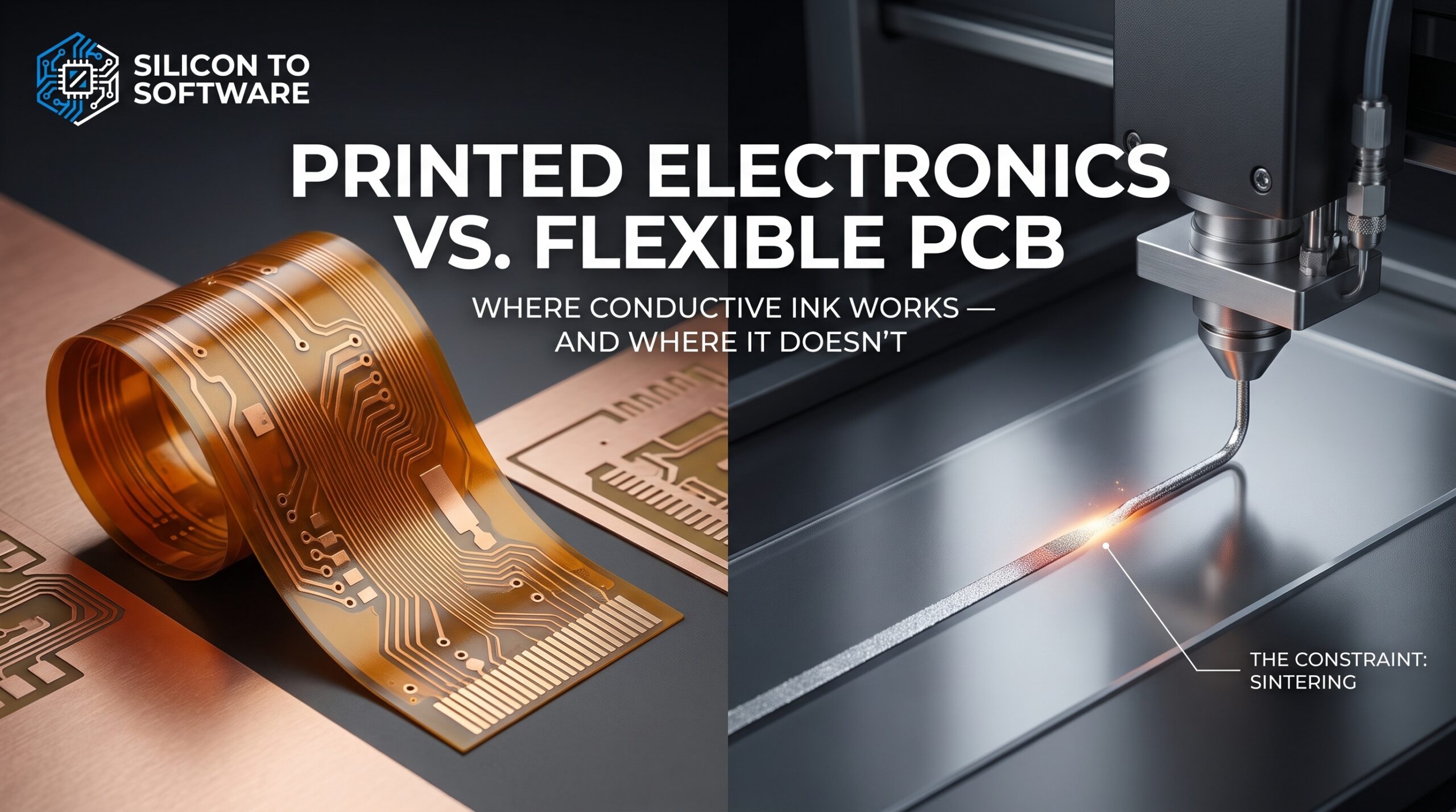
Printed Electronics vs. Flexible PCB: What Conductive Ink Can and Can’t Replace
-

Choosing the Right High-Speed Laminate for AI Hardware: Megtron 6 vs. Megtron 8 vs. Tachyon 100G
-

6G Technology Hardware: Why the Infrastructure to Build It Doesn’t Exist Yet
-

Satellite PCB Engineering in 2026: How AI, Radiation-Hardened Electronics, and Advanced Circuit Boards Keep Satellites Alive