Why US Chip Fabs Alone Won’t Fix the Electronics Supply Chain
The engineering reality behind substrate, packaging, and PCB fabrication — and why reshoring a fab doesn’t reshore a product
Table of Contents
A customer sent me a stackup last quarter — 16 layers, sequential microvias, tight registration tolerance, the works. He was thrilled. His company had just committed to sourcing the die from a US fab. “We’re finally bringing this home,” he told me.
Then he asked where I could get the board built.
I ran the numbers. At his volume and his tolerance requirements, there wasn’t a domestic shop that could touch it at a competitive price. The board — the actual thing his “domestic” chip was going to sit on — was going to Asia regardless of where the silicon came from.
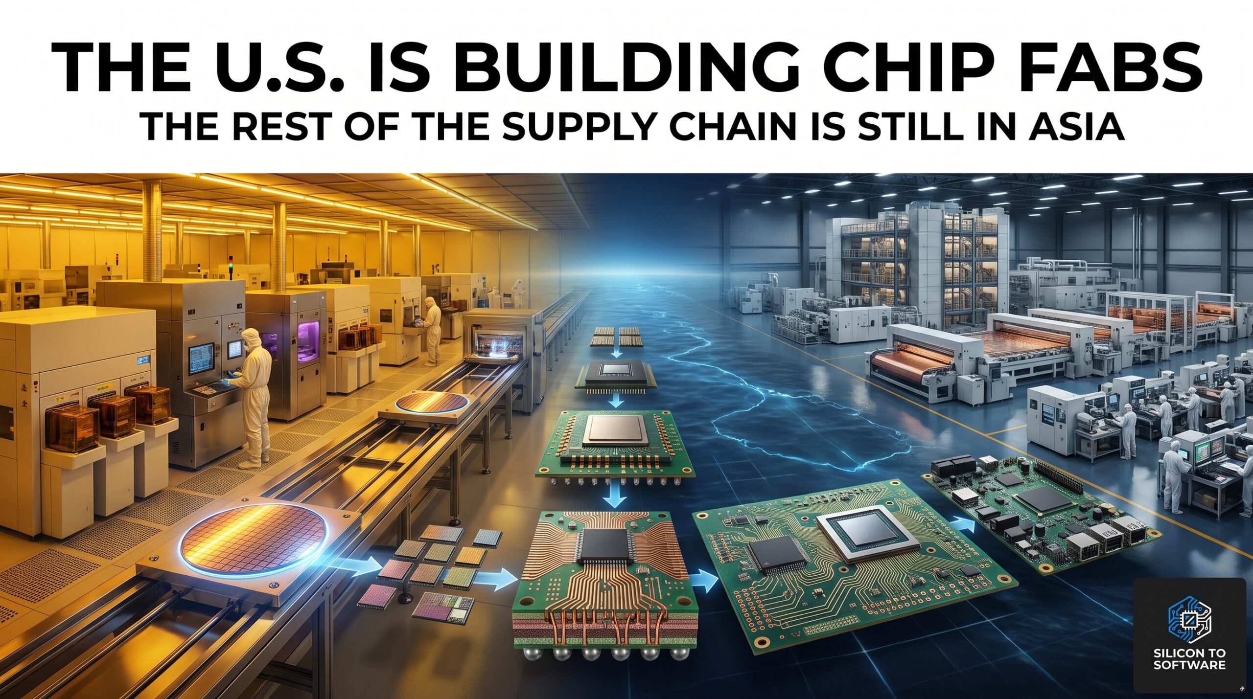
That conversation is the whole article in miniature. US chip fabs — Intel, Samsung, and TSMC have all committed tens of billions of dollars to advanced logic fabs on US soil — get treated in the headlines like a step toward chip self-sufficiency every time one breaks ground. But a fab is one node in a multi-stage manufacturing chain, and the nodes that turn a die into a finished, shippable product — wafer test, substrate, advanced packaging, PCB fabrication — haven’t reshored at anywhere near the same pace. This piece walks through where the current fab investments actually stand, what happens to a chip after it leaves the fab, and why the engineering constraints downstream — yield-learning curves, registration tolerance, process maturity — make this a much slower problem to solve than a construction timeline suggests. It also names the real, verified counterexamples: the places where domestic capacity genuinely is being built, and where it isn’t.
What US Chip Fabs Actually Deliver
Intel, Samsung, and TSMC have all committed tens of billions of dollars to advanced logic fabs in the United States, and the public record shows real, if uneven, progress. TSMC’s first Arizona fab entered high-volume production in late 2024 on its N4 process, with yield reported comparable to its Taiwan operations, and the company’s total Arizona commitment stood at $165 billion across six planned fabs, two advanced packaging facilities, and an R&D center as of this writing. TSMC has also acquired additional Arizona land and signaled room for further expansion beyond that count — I don’t have a formal primary announcement changing the committed six-fab number, so treat the $165B figure as a snapshot rather than a confirmed ceiling. Update: that $165B figure has since been superseded — in July 2026 TSMC raised its committed Arizona investment to $265 billion, adding two advanced-packaging facilities aimed directly at the downstream constraint this section flags. I break down what’s actually driving that packaging bottleneck in TSMC Arizona Bottleneck: A $265B Warning for AI Chips.
Intel’s Arizona fabs are further along than its Ohio site, where the company has pushed its production target back multiple times, from an original 2025 date to a current target in the 2030–2032 range. Samsung’s $17 billion Taylor, Texas fab (since expanded) was originally targeted for 2024 operation; as of mid-2026, the company states it remains on track for operational readiness in 2026, having previously delayed the project over a lack of committed customers.
Electrek reported in July 2026 that Tesla’s AI5 chip had reached tape-out and was scheduled for manufacturing at Taylor on Samsung’s 2nm process — a real milestone, but tape-out means the design is finalized and handed to the foundry, not that production samples are already coming off the Texas line. Multiple contemporaneous reports (TechTimes, Korea JoongAng Daily) place actual Taylor engineering samples as expected later in 2026, with volume production in 2027. I’m being precise about this distinction because I got it wrong in an earlier pass — I’d initially stated Taylor was “already producing” 2nm engineering samples, which overstates what the tape-out milestone actually means.
These are real, capital-intensive commitments, and they matter. But it’s worth being precise about what a fab produces: processed wafers. Those wafers still need to be tested, diced, and packaged before anything resembling a finished part exists — steps that, depending on the manufacturing flow, may or may not happen at the fab itself.
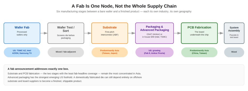
A fab does not produce a finished, shippable part. Between a bare die coming out of a fab and a working product on a shelf, several more manufacturing stages have to happen, each one its own specialized industry with its own geography:
- Wafer test/sort — electrically screening die on the wafer before anything gets packaged, so bad die don’t move downstream
- Substrate fabrication — the fine-pitch interconnect layer the die is mounted to
- Packaging, advanced packaging, and final test — die attach, wire bond or flip-chip, encapsulation, electrical test, plus the higher-end heterogeneous-integration processes (2.5D/3D stacking, chiplets, interposers, fan-out, hybrid bonding) that sit under the same broad stage; done either by outsourced assembly and test (OSAT) vendors like Amkor, or in-house by an IDM/foundry — Intel and TSMC both run their own advanced packaging lines, which is a meaningfully different model from OSAT
- PCB fabrication — the board that carries the packaged part into an actual system
- System assembly — populating and testing the finished board
Every one of these is a distinct manufacturing discipline with its own equipment, its own qualified suppliers, and its own geography. A fab announcement addresses exactly one of them. From a sourcing perspective, that’s the practical takeaway: a program manager tracking “fab progress” as the headline risk metric is watching the wrong stage. The schedule risk on a given program usually surfaces at whichever of these five later stages has the least qualified capacity — and that stage is rarely the one that got the groundbreaking ceremony.
The Substrate Bottleneck Nobody Photographs
Before a die ever touches a PCB, it typically lands on a substrate — a fine-pitch interconnect layer, often built with ABF (Ajinomoto Build-up Film) material, that fans the die’s fine pitch out to something a board can accept. This is the dominant pattern for advanced logic processors specifically; other device types use leadframe packages, wafer-level packaging, fan-out, or direct chip-attach approaches that skip a discrete substrate step entirely, so this section’s framing applies most directly to the CPU/GPU/HPC-class parts this article is centered on.
Substrates are today a distinct product category from HDI (High Density Interconnect) PCBs — related build-up and microvia techniques show up in both, but they’re different qualification paths, different feature-size regimes, and largely different supplier bases. That said, the line is starting to blur at the bleeding edge, and this isn’t a vague industry-trend claim — there’s a named technology for it. Substrate-Like PCB (SLP) construction borrows IC-substrate processes, most notably the modified semi-additive process (mSAP), and applies them at PCB panel scale, reaching fine-line geometries at or below 30 microns that sit between conventional HDI and true IC substrate capability.
TTM’s own SEC filings describe SLP as the next evolution beyond high-end HDI, built with mSAP; AT&S’s public materials confirm the same mSAP process applied across both its PCB and IC substrate lines. That’s two directly verifiable manufacturers straddling both categories — TTM being the same company named later in this piece for its Class 3 domestic Ultra-HDI work. Other manufacturers are named in industry technical write-ups as working in this same space, but I’ve only independently confirmed TTM and AT&S against primary company documentation, so I’m not extending the list further than that. Today’s qualification paths for mainstream ABF substrate and mainstream HDI PCB remain separate; SLP is the concrete evidence that the multi-year trajectory toward convergence is real, not speculative.
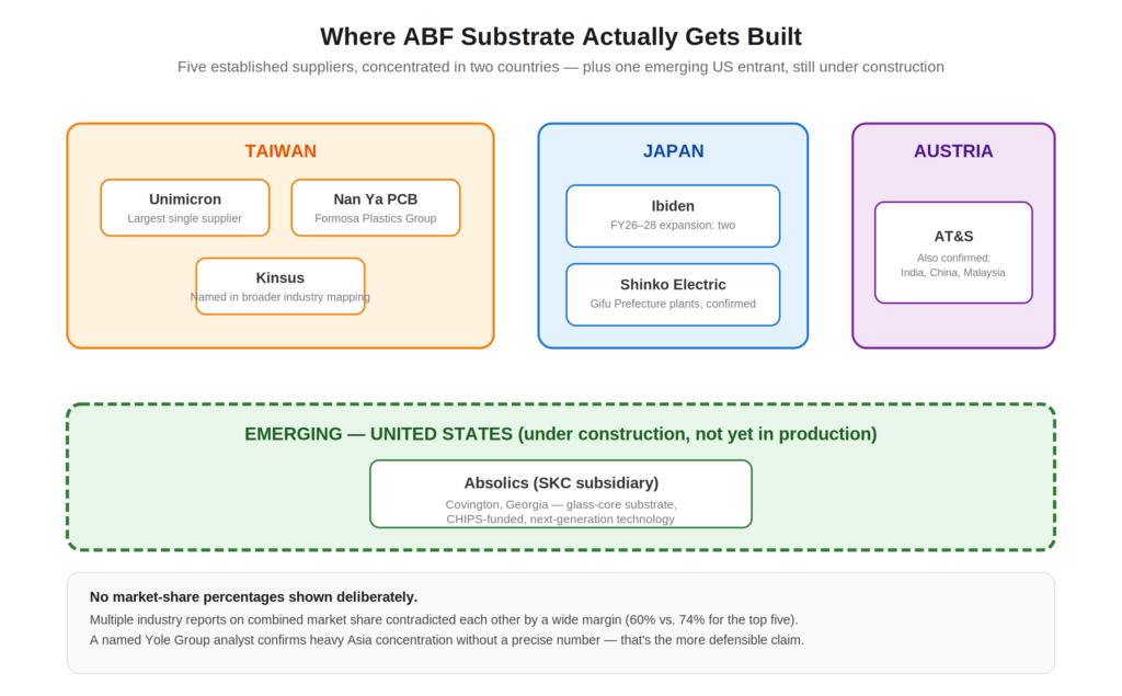
Substrate capacity is concentrated among a small number of suppliers, though it’s worth being precise about exactly how concentrated. Several industry reports place the top five ABF substrate suppliers — Unimicron, Ibiden, Nan Ya PCB, Shinko Electric, and AT&S — at a combined market share in the 60–75% range.
Digging further, though, reports from the same research firm contradict each other on the exact figure: one gives roughly 60% combined with no single supplier exceeding 18%; another from the same firm gives roughly 74% combined with Unimicron alone at 22%. That internal inconsistency is disqualifying for citing a precise number with confidence — and it’s likely compounded by an unstated scoping question none of these reports make explicit: whether the figures represent merchant-market share (substrate sold to outside customers) or total production including captive, in-house volume at IDMs like Samsung, which would move the numbers depending on definition.
What can be cited reliably instead is a named, on-record industry analyst. Bilal Hachemi of Yole Group — a genuine semiconductor-industry analyst firm — states that organic advanced IC substrate manufacturing “remains heavily concentrated in Asia, with dominant suppliers such as Unimicron, Ibiden, Shinko, Semco, and AT&S,” and that “U.S. and European players are beginning to respond with support from government programs such as the CHIPS Act, though they currently lag far behind in production capacity.” That’s a less quotable claim than a specific percentage, but it’s one that holds up.
During 2021–2022, ABF substrate shortages were a real, well-documented, and independent constraint on finished chip output — not merely downstream of wafer supply. Trade press reporting from that period recorded yield rates on high-end ABF substrate at major suppliers such as Unimicron running at roughly 70% or lower, with lead times stretching past 24 weeks, and Intel and Nvidia both co-investing directly in substrate suppliers’ capacity to secure supply.
That shortage eased by 2023–2024 as new capacity came online — but current institutional analyst forecasts reported by BigGo Finance, citing brokers covering Unimicron, Nan Ya PCB, and Kinsus, project the ABF substrate market shifting back into a supply-demand shortage by 2027, with the gap potentially reaching 29% by 2028, driven by AI/HBM-related demand growth outpacing roughly $19 billion in collectively announced supplier expansion plans. I’m naming the source explicitly because these are precise, specific figures, and precise figures need a named origin rather than a vague “analysts say.” So, the 2021–2022 crunch is history, but a comparable one is currently forecast within the next two to three years.
What the public record doesn’t establish, and what I can’t independently verify, is a precise comparison of substrate constraint versus wafer constraint in relative severity during 2021–2022 specifically — that framing is my own inference, not a stated finding I can point to. The underlying point stands regardless: substrate is its own chokepoint, gated by its own suppliers, independent of whatever wafer capacity exists.
On US substrate capacity, the picture is more complicated than a simple yes-or-no, in both directions. No verified evidence exists of Ibiden or AT&S building advanced ABF substrate fabrication capacity at scale on US soil. This is worth stating carefully: a widely-circulated claim about a specific Ibiden substrate fab under construction in Phoenix, Arizona, traces to AI-generated market-research content and does not hold up under a primary-source check. Ibiden’s disclosed fiscal 2026–2028 substrate expansion centers on two plants in Gifu Prefecture, Japan, and identifies no Phoenix, Arizona facility, and AT&S’s own site lists production only in Austria, India, China, and Malaysia.
A related, similarly unverifiable claim from the same source cluster — that Unimicron holds a stake in a Corning glass-substrate pilot line in New York — also doesn’t check out: Corning’s actual, primary-sourced New York investment (confirmed via New York’s governor’s office) is for photomask lithography glass, a different product entirely, with no mention of Unimicron anywhere.
Samsung Electro-Mechanics, whose own product page confirms production limited to South Korea and Vietnam, has no US site either, and the same is true of Nan Ya PCB, Shinko Electric, and Kinsus — no US capacity announcements found for any of them.
At the same time, there’s a real, verified example of emerging US substrate capacity worth naming specifically: Absolics, a subsidiary of Korea’s SKC, is building a glass-substrate facility in Covington, Georgia, confirmed by the US Department of Commerce’s own CHIPS Program Office — a 120,000-square-foot facility receiving up to $75 million in direct CHIPS Incentives Program funding, finalized December 2024, plus a separate $100 million CHIPS R&D award for glass-core substrate materials.
Commerce’s own announcement of that R&D award states plainly that these substrates “are not currently produced in the United States” — a primary-sourced government acknowledgment of exactly the gap this article describes, and evidence the gap is being worked on even where production-scale volume hasn’t arrived yet. Glass-core substrate is a next-generation technology distinct from the mainstream ABF material discussed above, so this doesn’t contradict the ABF-specific finding — it’s a separate, earlier-stage technology track worth tracking in its own right.
The physical mechanism: substrate lines are capital-intensive and require long qualification cycles — you don’t add meaningful capacity by flipping a switch, and you don’t requalify a new substrate supplier for a high-reliability part overnight.
The engineering trade-off: a new substrate line, wherever it’s built, commonly starts with lower first-pass yield than an established line running the same materials for over a decade, though the gap narrows faster when the transfer includes proven equipment and experienced personnel. That yield gap, where it exists, shows up directly in cost per good unit.
Practical consequence: a die fabricated on US soil can still be entirely dependent on the same handful of overseas substrate suppliers for the mainstream ABF material discussed above — though it’s worth noting Commerce is simultaneously funding several other early-stage US substrate and packaging research efforts (Applied Materials’ silicon-core substrate work, Arizona State’s advanced packaging research, Natcast’s piloting facility) beyond Absolics, so Georgia isn’t the only place this gap is being worked on, even if it’s the clearest example of a facility actually under construction.
The PCB Problem: Where the Chip Actually Lives
This is the part of the chain I spend my working life in, and it’s the part that gets the least attention in the reshoring conversation.
Advanced PCB fabrication — high layer count, HDI, sequential and stacked microvias, high or challenging aspect ratios — is concentrated overwhelmingly in Asia. Aspect ratio here means the ratio of hole depth to hole diameter for a drilled or laser-formed via; the higher that ratio climbs, the harder it gets to plate the barrel evenly, which shows up as thin spots prone to cracking under thermal cycling. High-aspect-ratio holes aren’t just “harder” in the abstract — they directly constrain achievable reliability, and they’re one more reason a line needs years of accumulated process history before it can run them at volume with acceptable yield.
Industry market research puts Asia-Pacific’s share of global high-end PCB production well above half, led by mainland China, Taiwan, and South Korea. The clearest single data point comes from TTM Technologies’ own SEC-filed 10-K, which cites Prismark Partners’ December 2024 industry report: worldwide PCB production in 2024 was approximately $73.6 billion, of which the Americas accounted for roughly 5% (about $3.4 billion) and China accounted for roughly 56% (about $41.0 billion), with the remaining 39% spread across the rest of the world.
That’s a materially different comparison than pairing a narrow “high-end PCB” subset figure against a broader global total — this uses one consistent dataset, one consistent scope. Worth being precise about what this is: it’s a public company’s SEC-filed 10-K citing Prismark Partners’ industry estimates, not an audited TTM financial figure in its own right. The filing is a stronger anchor than an unlinked market-research report, but the underlying numbers are still Prismark’s estimates, not something TTM’s auditors verified line by line.
The gap isn’t uniform across all PCB categories — it’s most acute at the advanced end of the spectrum, where layer count, via geometry, and registration tolerance push past what most domestic shops run at competitive volume.
Why Registration Tolerance Gatekeeps Sourcing Geography
Specification/observation: as stackups climb past 12–16 layers with sequential lamination and microvias, layer-to-layer registration tolerance becomes one of the major constraints — alongside minimum trace/space, laser-via geometry, microvia depth-to-diameter ratio, capture-pad geometry, and plated-via fill quality, all of which compound at this end of the spectrum. Registration is a useful lens for the rest of this section because it’s the one most directly tied to sequential lamination count, but it isn’t the only thing gating who can build these boards.
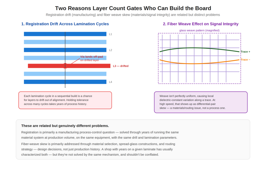
Physical mechanism: each lamination cycle in a sequential build introduces the possibility of misalignment between layers. Achieving tight registration across many lamination cycles requires process control refined over years of running the same material system — the same laminate, the same drill and lamination parameters, the same dimensional-stability behavior — at production volume.
A related but distinct issue is glass weave style: the weave pattern in a laminate’s fiberglass reinforcement isn’t perfectly uniform and can cause localized variation in dielectric constant along a trace’s length. On high-speed signals, that variation shows up as skew between differential pairs — the fiber weave effect — a real signal-integrity failure mode. It’s worth keeping these two issues separate: registration is primarily a manufacturing process-control question, while fiber-weave skew is primarily addressed through material selection, routing strategy, and design practice rather than production history alone. A shop with years of history on a given laminate has usually characterized both, but they’re not the same mechanism.
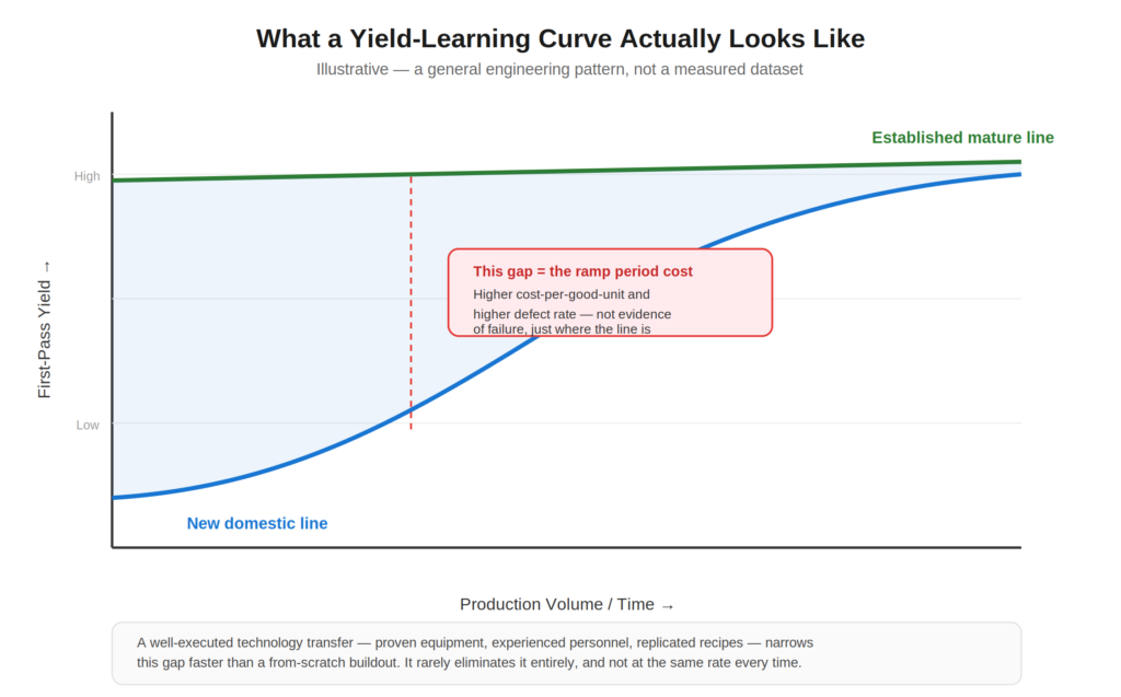
Engineering trade-off: an established Asian line with over a decade of process history on a given material system will hit tighter registration tolerance, at higher first-pass yield, than a newly stood-up domestic line running the same nominal process. The domestic line will get there — yield-learning curves do close over time — but during that ramp, cost and defect rate are both higher. That material-system dependency runs deeper than fab process alone, too — laminate selection itself is its own qualification challenge, with fab familiarity on a newer resin system directly affecting how fast a line can ramp to acceptable yield.
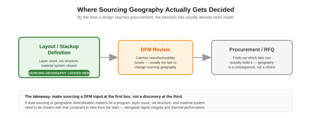
Practical consequence: for a large share of advanced board designs, sourcing geography isn’t really a choice made by procurement. It’s a choice made earlier, in the layout, the moment an engineer specifies a stackup that only a handful of fab houses on earth can build at volume.
This is also where IPC classification matters. IPC-6011 (Generic Performance Specification for Printed Boards) establishes three performance classes reflecting progressively more demanding requirements for functionality and continued performance: Class 1 for general electronic products, Class 2 for dedicated service electronics where enhanced performance is desired, and Class 3 for high-reliability electronics where continued performance or performance-on-demand is critical — including much military and aerospace product. It’s worth noting these classes are assigned by the applicable product specification and procurement requirements, not automatically by market sector — a consumer product isn’t automatically Class 1, and a defense product isn’t automatically Class 3. This piece is concerned almost entirely with Class 2 and Class 3, so Class 1 won’t come up again.
IPC-6012 applies qualification and acceptance criteria for rigid printed boards against those classes, working alongside IPC-A-600’s visual acceptance illustrations. The current revision, IPC-6012F, carries a September 2023 publication date on the standard itself and in the official standards store listings (electronics.org, ANSI, DIN Media all agree on September 1, 2023); the public press release announcing the revision followed about a month later, on October 18, 2023 — worth noting only because different secondary sources cite one date or the other depending on whether they’re referencing the document or the announcement about it. It expanded requirements addressing microvia-structure reliability and introduced test structures for evaluating complex interconnected-via constructions, among other updates directly relevant to the advanced HDI builds discussed here. (IPC itself was renamed the Global Electronics Association in 2025, though the standard numbering is unchanged.)
Domestic capacity for Class 3, high-reliability boards is a genuinely different — and smaller — conversation than commercial Class 2 volume capacity. Progress in one does not imply progress in the other, and coverage that conflates them overstates how far reshoring has actually come.
Why This Doesn’t Reshore on a Press-Release Timeline
None of this is a policy failure so much as a physical one. Yield-learning curves are not optional steps you can skip with enough capital.
A new production line — fab, substrate, or PCB — commonly starts its life at lower yield than a mature line running the same nominal process, though technology transfer that includes replicated equipment, proven recipes, and experienced personnel can substantially narrow that gap.
Yield improves as engineers tune process parameters against real production data: drill wander, lamination pressure and temperature profiles, etch consistency, registration drift. That tuning takes time and volume, and it doesn’t fully simulate in advance — TSMC’s own Arizona ramp, discussed earlier, is a reasonable example of how much a well-executed technology transfer can shrink this gap, even if it rarely eliminates it entirely.
The trade-off this creates: during the ramp period, a new domestic line can look more expensive and yield-limited compared to an established overseas competitor. That isn’t automatically evidence the reshoring effort failed — it’s a normal part of what a yield-learning curve looks like early on — but it’s also not guaranteed to happen at the same severity every time, and pretending it’s a fixed, universal law oversimplifies the engineering.
What Deserves Credit — and What’s Being Oversold
It would be dishonest to frame this as pure decline. Real progress exists, and it deserves to be named accurately — with real specifics, not vague gestures — rather than either inflated or ignored.
Advanced packaging and test capacity has seen genuine domestic investment, and two facilities are worth naming together, because they illustrate the two different models this work happens under. Intel’s Fab 9 in Rio Rancho, New Mexico, opened in January 2024 as the company’s in-house advanced packaging hub — Intel describes it as the only US high-volume advanced packaging site operating to date.
Amkor’s Peoria, Arizona campus, which broke ground in October 2025, is different: it’s an OSAT facility, built by a third-party packaging vendor rather than a chipmaker’s own operation, and Amkor describes it as the first US-based high-volume OSAT facility. Both claims can be true simultaneously — they describe different categories, in-house IDM packaging versus outsourced third-party packaging — and it’s worth naming both rather than letting one company’s “first” framing stand unqualified. For a program lead weighing sourcing risk, that distinction isn’t academic: capacity on an IDM’s captive line is tied to that one company’s own product roadmap and internal priorities, while capacity at an independent OSAT is shared across a customer queue that can be reprioritized on short notice when a larger customer’s order changes. Neither is strictly safer — they’re different risk profiles, and which one matters more depends on whether your bigger fear is one company’s roadmap shifting or a bigger customer bumping you in line. Treat this as a general sourcing-risk model, not a claim that every IDM or every OSAT behaves this way — the specifics vary by contract, customer tier, and facility.
Amkor’s committed investment has grown from an initial $2 billion to $7 billion across two phases, with 750,000 square feet of planned cleanroom space; construction is targeted for completion in mid-2027, with production beginning in early 2028. Apple has been named as Amkor’s first and largest customer, with Nvidia also named, and the facility is explicitly positioned to complement TSMC’s nearby wafer fabs. Between Fab 9 and the Amkor campus, both packaging models now have a domestic foothold — Fab 9’s has simply existed for longer than the pace of fab headlines might suggest.
Select domestic PCB fabricators serving mil-aero and other high-reliability Class 3 work have maintained — and in at least one case, actively expanded — capability through a period when commercial-volume Class 2 work migrated overseas. TTM Technologies is the clearest example. TTM opened a new 215,000-square-foot Ultra-HDI PCB manufacturing facility in Syracuse, New York, in June 2026 — purpose-built for exactly the high-layer-count, tight-tolerance work this article discusses. It’s a $130 million investment, including $30 million in direct Department of Defense funding, expected to add up to 400 jobs.
TTM describes itself, in its own investor materials, as America’s largest domestic manufacturer of advanced printed circuit boards. Its own FY2025 earnings presentation breaks out Aerospace & Defense at 44% of net sales — a precise, company-disclosed figure, not a third-party estimate. I don’t have an equally precise primary-sourced figure for what share of TTM’s manufacturing capacity specifically sits in North America versus its Asia facilities; that specific capacity split would need to come from TTM’s own segment disclosures rather than the revenue mix alone. This is real, substantial, verifiable domestic Class 3 capability, and it’s the strongest concrete counterexample to this article’s broader thesis found in researching it.
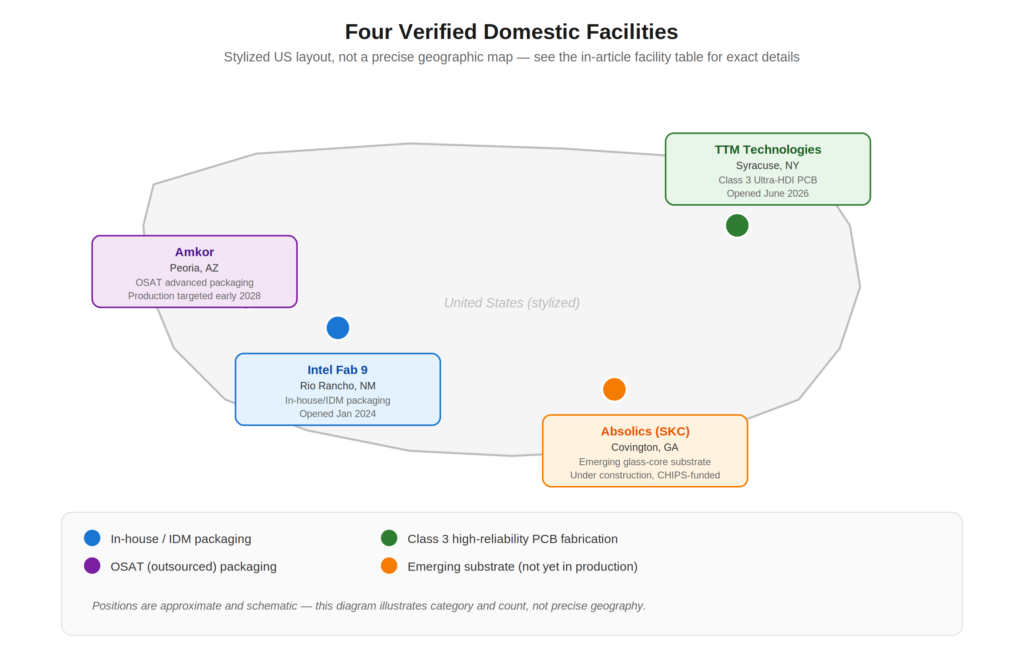
| Facility | Location | Category | Status |
|---|---|---|---|
| Intel Fab 9 | Rio Rancho, NM | In-house/IDM advanced packaging | Opened Jan 2024 |
| Amkor | Peoria, AZ | OSAT advanced packaging | Under construction; production early 2028 |
| TTM Technologies | Syracuse, NY | Class 3 Ultra-HDI PCB | Opened June 2026 |
| Absolics (SKC) | Covington, GA | Emerging glass-core substrate | Under construction; CHIPS-funded |
There’s also a stronger counterargument to this whole piece than a simple lead-time argument, and it deserves real sourcing rather than the weakest version. Two concrete mechanisms already exist that are specifically aimed at the gap this article describes.
First, CHIPS Act funding is not exclusively fab-focused: the Commerce Department’s CHIPS National Advanced Packaging Manufacturing Program finalized $1.4 billion in awards in January 2025, including $300 million specifically for advanced substrate and materials research split between Absolics, Applied Materials, and Arizona State University, plus $1.1 billion to operate a shared Advanced Packaging Piloting Facility.
Commerce’s own announcement of the Absolics award states plainly that the substrates it funds “are not currently produced in the United States” — a primary-sourced government acknowledgment of the exact gap this article describes, and a real rebuttal to any framing that policymakers have simply overlooked this node.
Second, the Department of Defense’s Trusted Foundry Program, managed by the Defense Microelectronics Activity (DMEA) since 2003, accredits suppliers across IC design, foundry, and packaging/assembly/test specifically to secure domestic and trusted sourcing for high-reliability microelectronics — a program that exists in the same broader space as efforts to keep counterfeit semiconductors out of defense and safety-critical supply chains, even though DMEA accreditation and counterfeit detection are distinct disciplines. DMEA’s own official accredited-supplier list stood at 78 suppliers as of November 2025, down slightly from 82 in early 2024, per DMEA’s own published lists (the count moves as accreditations are added or expire, so treat this as a point-in-time figure).
It’s worth being precise about what this program actually covers: DMEA’s published accreditation categories are IC design, aggregation, brokerage, mask manufacturing, foundry, post-processing, packaging/assembly, and test — a trusted-microelectronics and IC supply-chain framework. It is not the same thing as IPC Class 3 PCB qualification, and I have no documentation that TTM’s Syracuse facility specifically holds DMEA Trusted Supplier accreditation. The two programs are both relevant to domestic high-reliability electronics resilience, but they’re parallel mechanisms addressing different parts of the chain, not the same accreditation applied to two names.
A reader could reasonably conclude this problem isn’t overlooked so much as it’s being addressed through specific, dollar-figured, government-documented mechanisms. The more accurate reading is that these mechanisms still address a narrow slice of total volume — defense/aerospace procurement and early-stage R&D, not high-volume commercial production — and that the underlying yield curves and process maturity gaps don’t compress just because a funding mechanism or accreditation program exists. That’s a narrower, more defensible claim than “nobody is addressing this,” and it’s the fairer one to leave a reader with.
From Self-Sufficiency to Resilience
Full self-sufficiency — every node of the chain, onshore, for every product category — isn’t a realistic target, in my judgment, and treating it as the goal sets policy and procurement up to measure the wrong thing. I want to be direct that this is my own interpretation, not a conclusion the evidence in this piece independently establishes: what’s documented here is the specific gap between fab investment and downstream capacity; what follows from that gap — whether “resilience” is the more useful framing than “self-sufficiency” — is a policy judgment I’m offering, not a fact I’m reporting.
With that distinction stated, my own view is that resilience is the better framework: reducing single points of failure at the chokepoints that matter most, through genuine dual-sourcing and targeted domestic capacity where the risk is highest, rather than treating geography as an all-or-nothing scoreboard.
For engineers, this has a direct, actionable implication: sourcing strategy has to be a DFM input from the start of a design, not a question asked after the stackup is finalized — the same discipline covered in common PCB DFM mistakes that quietly kill fabrication yield applies just as much to knowing which fab can actually build what you’ve drawn, not just whether the geometry is technically producible somewhere.
If dual-sourcing or geographic diversification matters for a given program, the layout — layer count, via structure, material system — has to be chosen with that constraint in view alongside signal integrity and thermal performance. By the time a design reaches procurement with an exotic stackup already locked, the sourcing geography has usually already been decided.
What to Actually Watch
The next few years of coverage will keep producing fab groundbreaking headlines, and each one will carry the implicit promise that this is the moment the supply chain came home. It won’t be — not on its own.
What’s worth tracking instead is quieter and less photogenic: substrate capacity additions (watch Absolics’ Georgia ramp specifically, and whether ABF suppliers follow with anything comparable), advanced PCB fabrication investment at the HDI and microvia tier (TTM’s Syracuse ramp is the one to watch), and OSAT expansion (Amkor’s Peoria timeline) — the nodes that don’t get a ribbon-cutting ceremony but determine whether a domestically fabricated die can actually become a domestically built product. The tradeoff to track across all three is the same one: capacity announced versus capacity qualified at production yield — the gap between those two dates is where most of this timeline’s real risk actually sits.
A fab is a node, not a supply chain. The node everyone forgot to reshore was the board underneath the chip.
About the Author
Imran Valiani | Sales Director, PCB Electronics Manufacturing
20+ years working with major Bay Area and global tech clients. Founder of Silicon to Software, where I write about the hardware layer — PCB fab, AI gear, autonomous systems, and cyber — the stuff most tech writers have never touched. Literally.
Follow: X @SiToSoftware | LinkedIn
For more analysis of fabrication, DFM, materials, and manufacturing constraints, explore the PCB Manufacturing & Electronics Manufacturing Resource Hub.
This article was developed with AI assistance and edited, fact-checked, and reviewed by the author. See my full AI disclosure.
Sources
Company & investor disclosures
- TSMC Arizona official project page — tsmc.com/static/abouttsmcaz/index.htm
- Intel Newsroom — Fab 9 opening announcement, January 2024 — newsroom.intel.com/intel-foundry/intel-opens-fab-9-in-new-mexico
- Intel Newsroom — Ohio One construction timeline update — newsroom.intel.com/corporate/ohio-one-construction-timeline-update
- Samsung Semiconductor — Taylor, Texas fab corporate materials — semiconductor.samsung.com
- Amkor Technology — Peoria, AZ groundbreaking and $7B investment announcement — ir.amkor.com/news-releases/news-release-details/amkor-technology-breaks-ground-new-semiconductor-advanced
- Amkor Technology — original US advanced packaging and test facility announcement — ir.amkor.com/news-releases/news-release-details/amkor-announces-us-advanced-packaging-and-test-facility
- TTM Technologies — Syracuse, NY Ultra-HDI facility opening announcement — investors.ttm.com/news-events/press-releases/detail/407/ttm-technologies-opens-ultra-hdi-manufacturing-facility-in
- TTM Technologies — FY2024 Form 10-K (PCB market data citing Prismark Partners) — sec.gov/Archives/edgar/data/1116942/000095017025024839/ttmi-20241230.htm
- TTM Technologies — FY2025 earnings presentation (Aerospace & Defense revenue segment) — investors.ttm.com
- Ibiden Co., Ltd. — capital investment plan notice for high-performance IC package substrates, February 2026 — ibiden.com/company/2026/02/notice-regarding-capital-investment-plan-for-high-performance-ic-package-substrates.html
- AT&S — investor relations / production site listing — ats.net/en/investors
- Samsung Electro-Mechanics — package substrate product and production-site documentation — samsungsem.com/global/product/substrate/package-substrate.do
- Corning Incorporated / New York Governor’s Office — Corning Canton, NY investment announcement — governor.ny.gov/news/governor-hochul-announces-corning-invest-more-315-million-and-create-300-jobs-semiconductor
Government & regulatory sources
- US Department of Commerce — CHIPS National Advanced Packaging Manufacturing Program, $1.4B final awards announcement, January 2025 — commerce.gov/node/7087
- US Department of Commerce — Absolics CHIPS Incentives Program award announcement, December 2024 — commerce.gov/news/press-releases/2024/12/biden-harris-administration-announces-chips-incentives-awards-absolics
- Defense Microelectronics Activity (DMEA) — Trusted Supplier Program overview — acq.osd.mil/asds/dmea/tapo/trusted-supplier-programs.html
- DMEA — accredited Trusted Suppliers list, November 2025 — acq.osd.mil/asds/dmea/tapo/docs/tp/AccreditedSuppliers-03NOV2025.pdf
Standards organizations
- Global Electronics Association (formerly IPC) — IPC-6012F standard page — shop.electronics.org/ipc-6012/ipc-6012-standard-only/Revision-f/english
- Global Electronics Association — IPC-6012F release announcement — electronics.org/news-release/ipc-releases-ipc-6012f-qualification-and-performance-specification-rigid-printed
- Global Electronics Association — rename announcement, June 2025 — electronics.org/news-release/global-electronics-association-debuts-new-name-elevates-ipcs-70-year-legacy-voice-6-0
Industry analysts & trade press
- Yole Group — advanced IC substrate market press release (Bilal Hachemi quote) — yolegroup.com/press-release/pushed-by-glass-core-and-high-end-ics-substrates-for-ai-the-advanced-ic-substrate-market-reaches-31-billion-by-2030
- BigGo Finance — ABF substrate supply-demand gap forecast — finance.biggo.com/news/4978b0ef-fc31-4d7d-9de1-c14abbafc97b
- Electrek — Samsung Taylor / Tesla AI5 2nm tape-out report, July 2026 — electrek.co/2026/07/13/samsung-taylor-fab-tesla-ai5-chip-2nm
- TechTimes — TSMC Arizona fab profitability and production reporting
- DigiTimes, Tom’s Hardware, SourceEngine — 2021–2022 ABF substrate shortage contemporaneous trade press coverage