Edge AI Chips: The Future of AI Hardware and Why They’re Replacing Cloud-Based Intelligence
Edge AI chips are pulling artificial intelligence out of distant data centers and into the devices around you — compact processors, edge computing hardware, TinyML microcontrollers, and next-generation circuit boards making real-time intelligence possible anywhere.
Table of Contents
The 200-Millisecond Problem That Changes Everything
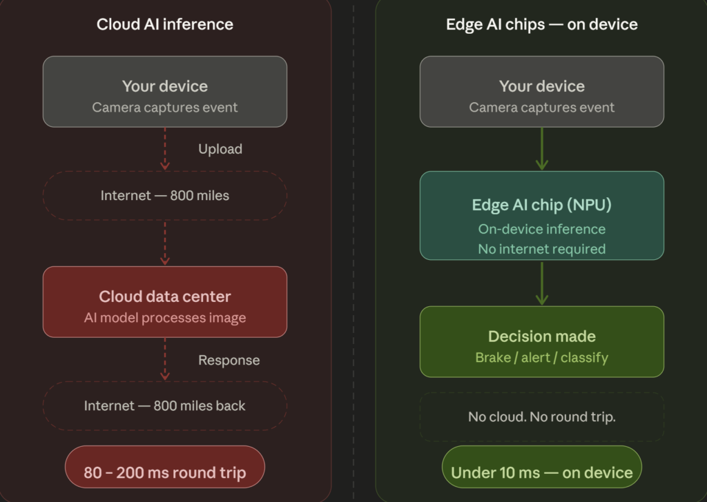
Picture this. A self-driving vehicle is doing 65 mph. A child runs into the road. The onboard camera catches it instantly — but here’s the problem — the edge AI chips that should be making the “brake now” call on-device aren’t there. Instead, the decision lives in a data center 800 miles away. That image has to travel up, get processed, then a response has to travel back. Under ideal conditions, a cloud round trip like this can burn somewhere between roughly 80 and 200 milliseconds — the actual figure varies with network path, geography, and congestion.
At 65 mph, your car covers approximately 95 feet every second. Do the math.
Roughly 8 to 19 feet. Gone. Before the brake command even starts its return trip. This scenario isn’t invented from thin air — latency-driven decision failure in autonomous vehicles is a documented engineering constraint, one that researchers and automotive OEMs have publicly cited as a core argument against cloud-dependent inference for safety-critical functions. The specific numbers vary by network and geography. The physics doesn’t.
Here’s the thing. That single scenario makes the entire argument for edge AI without a single chart or whitepaper. If your AI can’t think where the action is happening, it’s not really intelligent — it’s just an expensive lookup table with a latency problem.
What Is Edge AI, Actually?
Let’s kill the buzzwords fast.
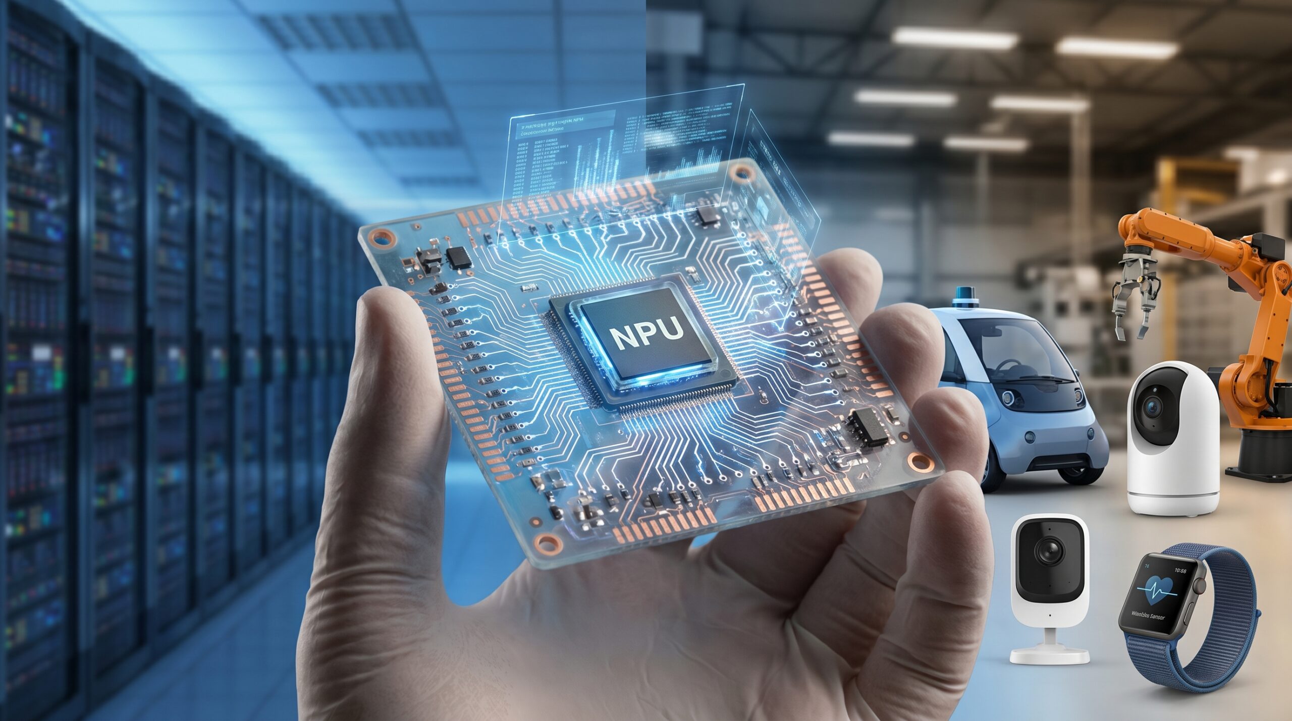
Edge AI means running AI inference directly on the device where data is collected — a car, a factory camera, a medical sensor, your phone — instead of shipping that data to a remote server somewhere. That’s it. That’s the whole thing.
The “edge” is a network topology term. Outermost layer. As far from the data center as you can get. When AI runs at the edge, you typically get three things a cloud round trip fundamentally cannot guarantee:
- Low latency — inference often completes in single-digit to tens of milliseconds on-device, removing the cloud network round-trip from the decision path entirely
- Data locality — sensitive information never leaves the device
- Offline resilience — the system keeps working when connectivity drops
I’ve found that most beginners assume edge AI is just a smaller version of cloud AI. Wrong framing. Edge AI isn’t a stripped-down cloud. It’s a different architectural philosophy entirely — you can see it deployed at scale in smart city infrastructure, where sensor nodes and 5G small cells depend on exactly this kind of on-device processing. Understanding that distinction is the first thing you need to get right.
Why the Cloud Model Is Hitting Its Limits
Cloud AI earned its dominance. Centralized GPU clusters — think NVIDIA’s H100, H200, and the newer Blackwell-architecture B200 Tensor Core GPUs — deliver computational horsepower that has no current edge equivalent. Training a large language model with tens of billions of parameters requires that scale today. Frontier-model training remains overwhelmingly dependent on large-scale data-center compute — that could shift over time as accelerator efficiency improves, but it’s the current state of the field.
But that’s training. The conversation has moved.
The real issue is inference at scale. Once a model is trained, running it for billions of real-world predictions creates problems the cloud was never built to solve.
The Bandwidth Wall
Global IP traffic has grown exponentially with every wave of connected devices — and generative AI workloads and IoT sensor networks have only accelerated that. Here’s what I want to be clear about, though: the problem isn’t that cloud infrastructure can’t scale. AWS, Microsoft Azure, and Google Cloud are spending hundreds of billions specifically to ensure it does. The actual problem is more specific and more annoying — cloud-first architectures become increasingly expensive, bandwidth-hungry, and latency-constrained for real-time edge workloads. Routing every sensor frame through a data center when the decision has to happen at the machine? Often economically and operationally impractical. Full stop.
The Privacy Reckoning
GDPR. CCPA. They’re tightening. Shipping raw biometric data, medical images, or financial transactions to third-party cloud servers creates compliance exposure that legal teams are increasingly unwilling to sign off on. Phone biometrics are the everyday example: Apple and Google both state that Face ID and Pixel face models stay on the device.
But to be honest with you, edge AI changes the threat model. It doesn’t eliminate it. Local inference still faces firmware compromise, supply-chain attacks, physical extraction, insecure OTA (over-the-air) update mechanisms, Differential Power Analysis (DPA), Fault Injection (FI), and model theft via side-channel analysis. These aren’t hypothetical — self-driving cars already have documented hardware security gaps in exactly this threat category. Moving intelligence to the edge shifts where you have to defend, not whether you have to defend. For engineers designing these systems, that distinction matters enormously.
The Economics Don’t Scale
Cloud inference costs money per query. Every single one. For a consumer app sending millions of API calls per day, that adds up fast (uncomfortably fast, if you’ve ever seen a cloud bill mid-scaling event). Running inference locally on dedicated silicon has a one-time hardware cost, with marginal per-inference costs driven mainly by device power draw — plus the ongoing cost of firmware maintenance, security patching, and fleet management, which is real but generally lower than recurring cloud API fees at meaningful scale. The TCO (Total Cost of Ownership) math tends to favor edge deployment at volume, though the full comparison depends on deployment scale, connectivity costs, and device lifecycle.
Meet the Edge AI Chips Making This Possible
This is where it gets genuinely interesting.
Neural Processing Units (NPUs)
The NPU is the workhorse. Unlike a CPU (general-purpose) or a traditional GPU (parallel graphics and compute), an NPU is purpose-built for the matrix multiplication and tensor operations — including activation functions and, in transformer-based models, attention computation — that account for the bulk of neural network inference workload.
Apple’s Neural Engine has been integrated into A-series and M-series chips since the A11 Bionic. Apple states the M4 chip’s Neural Engine delivers up to 38 TOPS (Tera Operations Per Second). Apple doesn’t publish the precision methodology behind that figure in consumer materials, and independent technical analysis has found that Apple’s “38 TOPS” is calculated by doubling the chip’s FP16 throughput to represent an INT8-equivalent rate — a common industry convention — rather than a directly measured INT8 benchmark. That’s a meaningful methodology detail: it means the advertised figure represents a theoretical scaling, not a hardware-measured result at that precision.
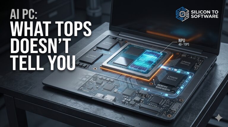
Qualcomm’s mobile flagship, the Snapdragon 8 Elite, includes a dedicated Hexagon NPU built for on-device inference in Android smartphones. Qualcomm’s own Snapdragon 8 Elite product brief describes the Hexagon NPU as “45% faster” than its predecessor — a relative performance claim, not an absolute TOPS figure. The “45 TOPS” number that circulates around this generation of Qualcomm silicon is officially Qualcomm’s figure for the Snapdragon X Elite, a separate PC/laptop platform — not the Snapdragon 8 Elite phone chip. These are two different products from the same architecture family, and the TOPS figures aren’t interchangeable. This is exactly the kind of mix-up that makes vendor-to-vendor TOPS comparisons unreliable without checking the specific platform and precision behind each number. Use these figures for directional comparison. Not absolute benchmarking. For the laptop-specific version of this problem — Microsoft’s 40 TOPS Copilot+ threshold, and how Intel, AMD, and Qualcomm’s ratings compare — see my breakdown of AI PC NPUs.
Here’s the engineering reason that caveat matters. Every AI workload has two separate requirements running at the same time: a compute requirement — how many multiply-accumulate operations it needs — and a data-movement requirement — how many bytes have to move between memory and the compute array to make those operations happen. Engineers describe the ratio between the two as arithmetic intensity: compute operations per byte moved. It’s the same concept behind the roofline model used across chip architecture analysis.
High arithmetic intensity means the compute array is more likely to be the limiting factor — there’s plenty of data on hand, and the NPU stays busy. Low arithmetic intensity means the opposite. The compute array sits idle, waiting on memory to deliver the next batch of weights or activations. In that second case, a chip’s advertised TOPS ceiling never actually gets reached, no matter how much raw compute sits on the die.
The relationship is simple to state, even if the real-world math gets more involved: real performance is capped at whichever ceiling the workload reaches first —
Achievable performance ≤ min ( Peak Compute, Memory Bandwidth × Arithmetic Intensity )
This isn’t a benchmark or a vendor claim — it’s the general shape of the constraint. To make it concrete with an illustrative, non-vendor-specific, hypothetical example: imagine a chip rated at 100 TOPS peak. If the workload running on it has low arithmetic intensity — lots of data movement relative to compute, common in certain transformer inference patterns — the memory subsystem may only be able to feed the compute array fast enough to sustain a small fraction of that 100 TOPS figure. Same silicon. Same rated peak. Very different real-world number, because the limiting resource shifted from compute to memory bandwidth.
This doesn’t mean memory is always the bottleneck, or that TOPS figures are meaningless — plenty of workloads are genuinely compute-bound, and peak TOPS remains a useful measure of ceiling capability. But it does mean the question that actually matters at the edge isn’t “how many TOPS does this chip advertise?” It’s whether the memory subsystem — and the power and thermal envelope surrounding it — can keep that compute array fed for the specific workload you’re running. Edge platforms often have tighter memory bandwidth, memory capacity, power budgets, and thermal budgets than a data center accelerator. That makes this question more consequential at the edge than almost anywhere else in the AI hardware stack.
The RISC-V Factor
Here’s something most tech coverage underreports. RISC-V — an open-source instruction set architecture — is gaining real traction for custom edge AI silicon, particularly among startups and Chinese semiconductor firms. The RISC-V ISA itself carries no license fee to use. That said, “no licensing fees” oversimplifies the real picture: commercially licensed RISC-V IP cores from vendors like SiFive, Codasip, and Andes do carry their own licensing costs — you’re paying for the microarchitecture implementation and support, not the ISA itself. ARM, for its part, also licenses under multiple models (architecture licenses, core licenses, royalty structures) rather than one flat fee. The real cost advantage of RISC-V is the option to avoid ISA-level royalties entirely if you build or use an open-source core — that’s genuine, but it’s a narrower claim than “no fees, period.”
To be straight about it, though: ARM still dominates production-grade edge AI today. RISC-V adoption is real and growing — some industry estimates project a rising share of the market over the next few years — but it hasn’t overtaken ARM’s install base. The architectural freedom is genuine — the software ecosystem, the compilers, the production-tested AI toolchains, they’re still maturing relative to ARM’s infrastructure. That gap is closing. It hasn’t closed.
TinyML: AI in the Smallest Possible Package
TinyML is the discipline of running machine learning models on microcontrollers with extremely limited resources — often less than 1 MB of RAM, power budgets ranging from sub-100 microwatts for always-on tasks like keyword spotting up to a few milliwatts for more complex classification work.
Frameworks like TensorFlow Lite (Google) and Edge Impulse let developers deploy compressed, quantized neural networks on devices like the Arduino Nano or STM32 microcontrollers. To be honest, the first time I saw a keyword spotting model running on something smaller than a postage stamp consuming microwatts of power, it recalibrated my entire sense of what “AI hardware” even means.
Scale-wise: a 2021 ABI Research baseline (circulated via the TinyML Foundation) estimated over 2.5 billion TinyML-capable device shipments by 2030. That’s a five-year-old projection at this point — treat it as a directional industry baseline established early in the category’s growth, not a current or updated forecast. The more durable point is simpler. TinyML deployments are generally understood to be counted in the billions of units, placing them among the largest categories of AI inference endpoints in existence.
The PCB and Systems Engineering Behind Edge AI Chips
Here’s what most blog posts skip entirely.
Deploying an NPU or edge AI accelerator isn’t a software problem. Not primarily. The hardware integration challenges are real — and they start with the board.
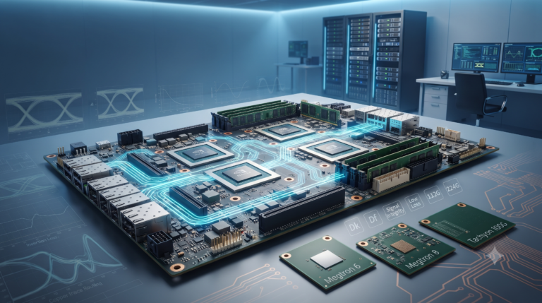
Edge AI chips designed for high-speed inference require PCBs built to tight electrical specs. High-Density Interconnect (HDI) PCB designs fall under IPC-2226 — the Sectional Design Standard for High Density Interconnect Printed Boards — which provides design guidance for via structures, trace densities, and layer stackups appropriate to high-density routing. The standard sets the design framework; it doesn’t prescribe a universal layer count or via geometry — actual stackup, routing density, and via structure are determined by the specific board design, driven by the signal count and pitch of the components being routed. IPC-A-600 governs finished board inspection. Different documents. Different functions. Conflating them is a common error in non-specialist coverage (I’ve seen it in vendor briefs, not just blog posts). If you’re evaluating PCB materials for AI hardware more broadly, comparing high-speed laminates like Megtron 6 vs. Megtron 8 is the next layer of that engineering decision.
Thermal management is where things get genuinely complex. Thermal vias and copper planes form the PCB-level foundation for heat dissipation. NVIDIA states the Jetson AGX Orin module delivers up to 275 TOPS with power configurable between 15W and 60W depending on the selected power mode — the higher end of that range is where sustained inference workloads push the hardest. At that power level, thermal vias alone aren’t enough. System designers typically add heat spreaders, vapor chambers, thermal interface material (TIM) optimization, and, in some deployments, forced airflow. Thermal simulation before hardware release is standard practice for any high-power sustained edge AI integration, though the depth of simulation required varies with power level and enclosure constraints. The circuit board is the starting point, not the complete solution.
Here’s what happens if that cooling isn’t enough. Running an NPU at full compute load draws power, and that power has to go somewhere — it becomes heat. As junction temperature climbs toward the chip’s rated limit, the processor’s power management logic steps in and protects the silicon through thermal throttling: it reduces clock speed, reduces voltage, or both — a mechanism generally referred to as dynamic voltage and frequency scaling, or DVFS. The exact throttling behavior varies by chip and vendor implementation, but the underlying principle is consistent: the chip doesn’t fail; it gets slower automatically to stay within a safe operating temperature.
This is why peak TOPS and sustained TOPS are two different numbers. A chip can hit its advertised performance for a period, then throttle down once junction temperature approaches its limit, settling into a lower sustained rate for the rest of the workload. Peak performance is not sustained performance — they describe two different operating conditions of the same silicon. For a burst inference task — a single camera frame, a one-shot classification — that distinction rarely matters. For continuous inference — a factory line running defect detection all shift, or a robot processing video nonstop — sustained performance is the number that actually matters, not the spec-sheet peak.
This is also where edge deployment gets genuinely harder than data center deployment. A rack-mounted accelerator has room for a large heatsink, high-volume airflow, sometimes liquid cooling, and substantial electrical infrastructure behind it. An edge module bolted into a drone, a car, or a compact industrial enclosure often doesn’t have any of that. Limited enclosure volume. Frequently passive cooling. Small heat spreaders. Restricted airflow. Battery power instead of a wall circuit. And ambient temperature that isn’t a controlled server room — it’s whatever the factory floor or the engine bay happens to be that day.
Push more compute density into a smaller edge enclosure, and you’re not really solving a compute problem anymore. You’re solving a thermal engineering problem. Burst performance versus sustained performance, and compute density versus thermal headroom — these are two of the defining trade-offs of edge AI hardware design, and they’re easy to miss if you’re only looking at the TOPS number on a spec sheet.
Memory bandwidth. Critical. Edge AI chips today commonly run LPDDR5 or LPDDR5X — low-power variants for mobile applications — though the specific memory architecture varies by chip family and design. LPDDR6 is beginning to emerge in higher-performance platforms, and some custom edge accelerators use proprietary memory hierarchies entirely. Edge devices are generally not designed around HBM2e or HBM3 stacked memory — that class of memory is more commonly associated with data-center and high-performance accelerator designs, largely due to power, packaging, and cost considerations — but this is a strong industry tendency rather than an absolute rule; specialized edge accelerator designs can and do vary.
That memory interface doesn’t stay a silicon-level decision — it propagates straight into the board, and this is the connection most coverage skips. A modern AI SoC paired with LPDDR5X often needs the memory device placed physically close to the package because signal integrity, timing margins, routing length, and power delivery all get harder as that distance grows. Getting the high pin count of that memory interface out from underneath a dense BGA package — the actual escape routing — is where the physical difficulty shows up. Depending on the package, memory configuration, and overall board architecture, that pin density can require tighter trace and via geometry than a standard PCB stackup can efficiently accommodate.
This is exactly the kind of problem HDI exists to solve. Microvias and higher routing density can provide additional escape paths within the same board area when conventional via structures can’t efficiently support the package breakout. That routing density doesn’t come free, though. It can increase stackup complexity, tighten layer-to-layer registration requirements, and add via-process steps a simpler board wouldn’t need — all of which can affect fabrication difficulty, inspection burden, manufacturing cost, and in some cases yield sensitivity. Not every edge AI board needs this treatment — a low-bandwidth microcontroller-class design typically won’t — but for higher-bandwidth NPU- and SoC-class designs, this is a real and underexplained consequence.
None of this is a software problem. It starts as an AI architecture decision — how much memory bandwidth the model needs — and it can end as a PCB manufacturing decision. Higher memory bandwidth requirements can drive more demanding physical memory interfaces. More demanding interfaces can drive tighter package and routing constraints. Tighter routing constraints can drive more complex PCB structures. More complex PCB structures can increase manufacturing difficulty and cost. That’s the chain IPC-2226 provides design guidance for — precisely because modern AI accelerator memory interfaces often push boards toward this level of density. IPC-A-600 then governs whether the finished board built to that design actually meets acceptance criteria. Two different problems — one upstream in design, one downstream in inspection.
The Industrial Edge: Where This Is Already Deployed
Edge AI is in factories today.
AI-powered vision systems running on FPGA-based edge accelerators (Xilinx, now part of AMD, is a major vendor here) inspect products at line speeds cloud latency simply cannot support. Think about it: a conveyor belt moving at 2 meters per second cannot wait 150ms for a cloud API to return a defect classification. The decision has to happen in under 10ms. Stop the line or pass the part. No round trip.
NVIDIA states the Jetson AGX Orin module delivers up to 275 TOPS (at INT8, with sparse compute optimizations), with power configurable between 15W and 60W. NVIDIA markets Jetson AGX Orin as deployed in robotics, autonomous machines, and industrial inspection applications. This same edge AI hardware category is also central to the hardware gaps holding back humanoid robots on factory floors — a related deployment challenge worth understanding. One thing worth flagging: NVIDIA continues to evolve the Jetson roadmap — always verify current platform specs against NVIDIA’s published product pages before committing to a design, since figures and power modes have shifted across firmware and software updates even on existing hardware.
What This Means for You as a Beginner
So where does this leave someone just starting to understand this space?
A few honest observations — and I mean honest, not the usual “here are five takeaways” list:
- Cloud AI and edge AI aren’t opponents. Training happens predominantly in the cloud today. Inference is increasingly moving to the edge. That division of labor is the most useful mental model you can build right now.
- The chip companies to watch are NVIDIA (Jetson line), Qualcomm (Snapdragon and Cloud AI series), Apple (Neural Engine), Google (Edge TPU), and a growing cohort of startups including Hailo, Kneron, and Syntiant. On the automotive side specifically, Tesla’s FSD chips and the broader shift toward AI-powered vehicles show this same architecture playing out in cars. (No commercial relationship with any vendor listed above. All mentions are based on publicly available information and independent editorial judgment.)
- Software frameworks matter as much as hardware. TensorFlow Lite, PyTorch Mobile, and ONNX Runtime are the primary tools for deploying models at the edge. Know these names. They give you a vocabulary for the conversation.
- TOPS-per-watt is often a more useful comparison than raw TOPS. In edge AI, an AI chip delivering 50 TOPS at 5 watts can be more valuable in a battery-powered device than one delivering 100 TOPS at 25 watts, depending on the workload. Raw TOPS alone is frequently the wrong metric to lead with. Power efficiency is often the more relevant competition.
This field moves fast. For latency-sensitive workloads, intelligence that lives close to where decisions must be made typically outperforms architectures that depend on a remote server rack a thousand miles away.
The cloud gave us AI at scale. Edge chips are giving us AI at speed.
About the Author
Imran Valiani | Sales Director, PCB Electronics Manufacturing
20+ years working with major Bay Area and global tech clients. Founder of Silicon to Software, where I write about the hardware layer — PCB fab, AI gear, autonomous systems, and cyber — the stuff most tech writers have never touched. Literally.
Follow: X @SiToSoftware | LinkedIn
For more analysis of compute, power, cooling, and infrastructure constraints, explore the AI Hardware & Data Centers Resource Hub.
This article was developed with AI assistance and edited, fact-checked, and reviewed by the author. See my full AI disclosure.
Sources
- Apple — M4 Chip Introductory Brief: apple.com/newsroom/2024/05/apple-introduces-m4-chip
- Apple M4 Neural Engine independent benchmark analysis: maderix.substack.com — “Inside the M4 Apple Neural Engine”
- Qualcomm — Snapdragon 8 Elite Product Brief: qualcomm.com
- Qualcomm — Snapdragon X Elite Product Brief (45 TOPS figure source): qualcomm.com
- NVIDIA — Jetson AGX Orin Product Page (275 TOPS, 15–60W power range): nvidia.com/en-us/autonomous-machines/embedded-systems/jetson-orin
- ANSI Webstore — IPC-2226A-2017: webstore.ansi.org/standards/ipc/ipc2226a2017
- RISC-V International Foundation FAQ (licensing): riscv.org/about/faq
- EU GDPR: gdpr.eu
- California CCPA: oag.ca.gov/privacy/ccpa
- ABI Research / TinyML Foundation 2021 baseline: tinyml.org
- NVIDIA — Blackwell Architecture & B200: nvidia.com/en-us/data-center/b200
- IPC — Design and Inspection Standards Overview: ipc.org/ipc-design-standards