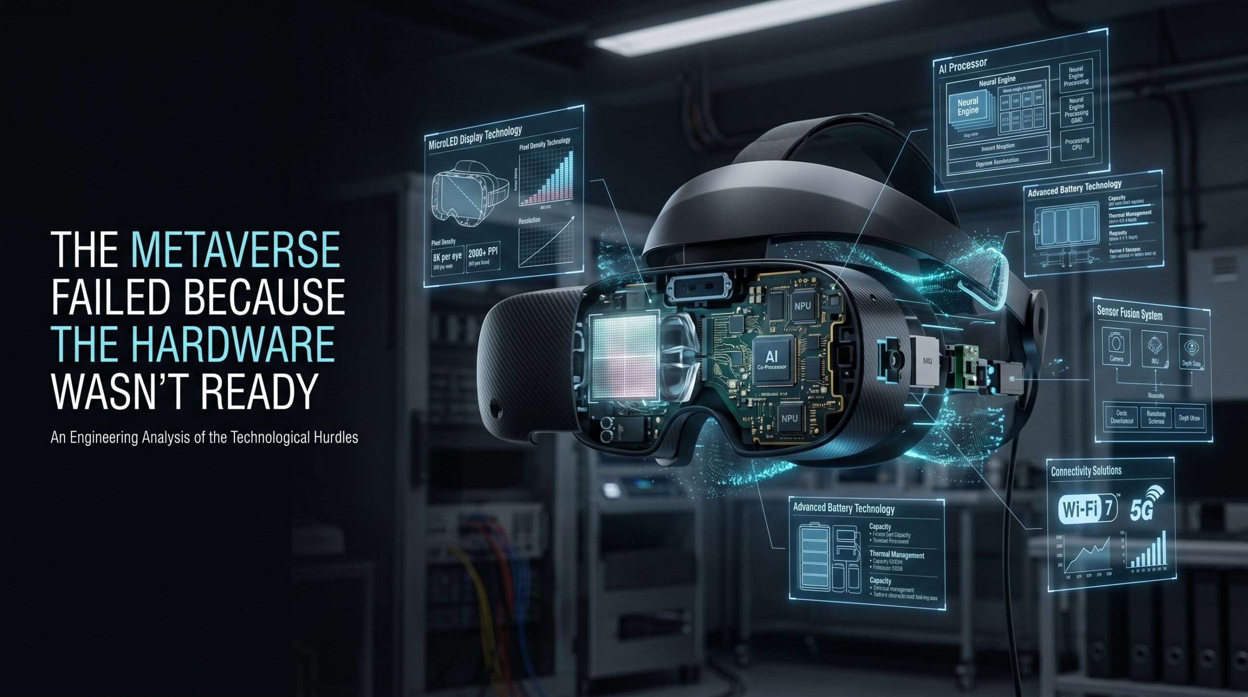
6 Metaverse Hardware Failures That Killed the Dream — And What Needs to Change
The next wave of spatial computing lives or dies on metaverse hardware: chips, screens, cells, sensors, AI acceleration, and the wireless pipes that tie them together.
Table of Contents
Let me start with a number that still blows my mind. $19.2 billion. That’s what Meta’s Reality Labs lost in 2025 alone — just that one year. The year before? $17.7 billion. Before that: $16.1 billion, $13.7 billion, $10.2 billion, $6.6 billion, going back to 2020. All told, $83.6 billion in the hole by the end of 2025, per Meta’s own filings. Every dollar of it spent trying to solve a metaverse hardware problem the industry wasn’t ready for.
The press had a field day. “Proof the metaverse was a fever dream.” “Zuckerberg’s folly.”
They missed the point entirely.
The money didn’t fail. The vision didn’t fail. At the end of the day, the metaverse hardware stack — the screens, the chips, and the cells — just couldn’t do what the vision asked of them.
I’ve seen this exact pattern — not in headsets, but in the PCB supply chain I’ve worked in for over 20 years. A client draws up a roadmap. It’s bold, it’s exciting. Then the substrate guys tell you what they can actually yield at volume. Those two things are almost never the same. The metaverse didn’t ship broken. It shipped before the stack was ready.
I know what you’re thinking: “Isn’t that just an excuse?” Maybe. But there’s a real difference between a bad idea and a good idea with bad timing. I think the metaverse is the second one.
Metaverse Hardware Problem #1: Screens Nobody Could Actually See Through
Here’s something I’d skip in a board meeting but won’t skip here: the display problem was obvious to anyone who’d ever put on a first-gen VR headset. You see the screen-door effect immediately — that weird grid between pixels that your brain reads as “fake.” Not a software bug. Not a settings issue. Just physics.
Apple’s Vision Pro knocked that problem down hard — high-density micro-OLED panels; most reviewers couldn’t spot the screen-door effect at all. Good. Not great. The Vision Pro still lands around 34 PPD (pixels per degree), per independent display analyses based on Apple’s published specs (7.5 µm pixel pitch, 23 million pixels — Apple doesn’t publish the PPD figure directly, worth noting).
The human eye wants closer to 60 PPD in the center of your field, under commonly cited XR display models — though I’ve seen published estimates run anywhere from 57 to 70+ PPD depending on what assumptions you plug in. Per display research from the Society for Information Display (SID), early consumer VR shipped at 15–20 PPD. So we’ve come a long way. Not far enough.
What does “far enough” actually require?
- ~60 PPD in the foveal zone — that’s the threshold the industry calls “retinal display” quality
- Wide field of view (FoV) — at least 100–120 degrees horizontal
- High refresh — 90Hz floor, 120Hz is where you want to be, to prevent vestibulo-ocular reflex (VOR) mismatch (the technical name for “wearing this thing made me want to lie down”)
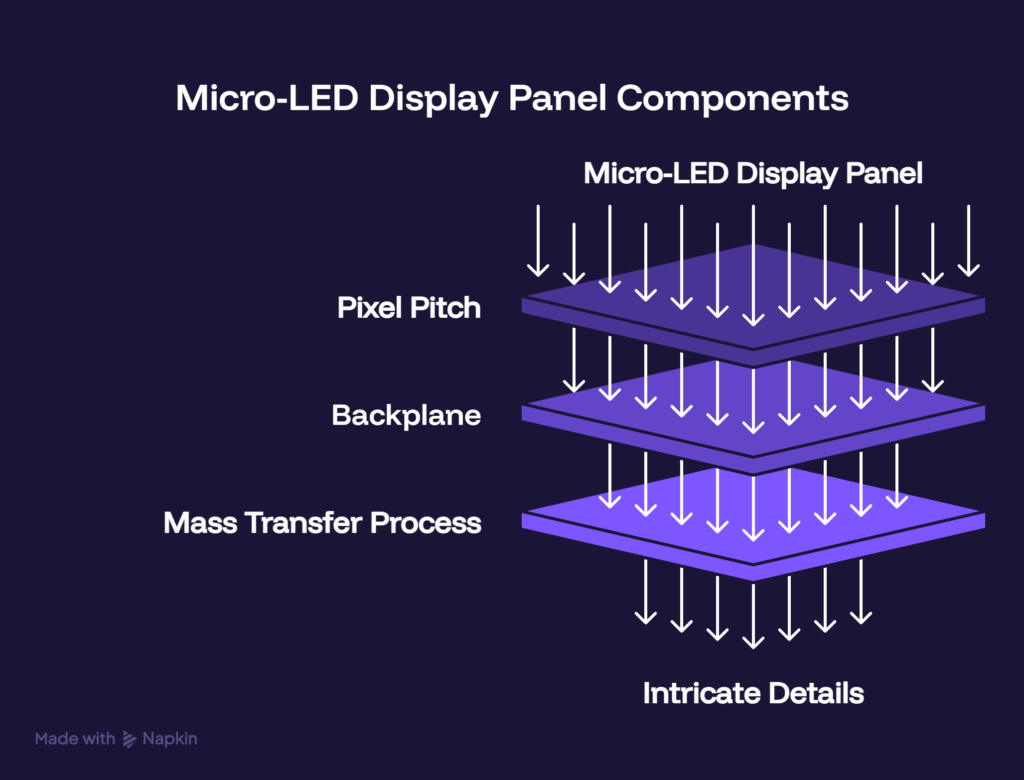
Hit all three in a package someone will actually wear for two hours? That needs pixel pitch densities and display substrates that exist in labs right now — just not at anything close to consumer-scale cost and yield. Not pessimism. Fab economics.
The play is micro-LED (μLED). Brighter and faster than OLED or LCD, with a power-efficiency advantage that hasn’t yet shown up in shipping products. The snag is mass transfer yield — moving millions of tiny LED chips onto a backplane with acceptable defect rates is genuinely hard. (Here’s why MicroLED is so hard to manufacture.)Transfer accuracy, defect repair, epitaxy uniformity, wafer bonding, color conversion — none of these are unsolved science, but none of them are cheap to solve at scale either. Apple, Samsung Display, LG Display all have programs. Timelines for cost-competitive consumer HMD production? Still anyone’s guess.
On the other hand, maybe I’m wrong about the timeline being that far out. The industry surprised everyone with OLED. Could happen again.
Metaverse Hardware Problem #2: The Chip That Can’t Stay Cool
I’m going to start with the thing that actually matters and work backward. A desktop GPU for VR eats 300–450 watts. Your headset’s chip gets maybe 5 to 15 watts. That gap is the whole story, honestly.
Why the SoC Is a Thermal Problem Disguised as a Performance Problem
The Quest Pro ran on Qualcomm’s Snapdragon XR2+ Gen 1. The Quest 3 stepped up to the Snapdragon XR2 Gen 2 — real gains in graphics and AI inference. Different chip. Better numbers. Same fundamental ceiling: mobile SoC architectures built for phones, running hot against your face, with nowhere for the heat to go.
The thermal budget is fixed. No software patch changes that.
Here’s the rendering workload you’re asking that 10-watt chip to handle:
- 6DoF (six degrees of freedom) tracking — head position and rotation computed across three translational and three rotational axes, in real time
- Passthrough mixed reality — camera feeds composited with under 10ms motion-to-photon latency
- Foveated rendering — cutting resolution outside your current focal point to save compute cycles
- Real-time physics and spatial audio — because the world needs to feel real, not just look real
Run that stack simultaneously, and you get a headset that throttles, runs warm, and dies in a couple hours. Not great.
I’ve noticed that most hardware coverage stops at “the chip wasn’t fast enough.” That’s not quite right. The chip might be fast enough. The thermal path isn’t. A headset sits against your skin — you can’t cool it like a server. The Vision Pro and Quest Pro both have small fans. Still not enough.
Passive management (graphite heat spreaders, vapor chambers, PCB layout discipline) carries most of the load. That’s what actually caps the SoC’s sustained Thermal Design Power (TDP) in real-world use. The silicon might handle 15 watts under full load. The thermal path to ambient in a lightweight headset often can’t shed that heat on a continuous basis.
To be honest, I’d argue thermal engineering is the most underrated problem in the entire XR stack. Everyone argues about specs. Nobody wants to fund vapor chamber R&D.
What needs to change? Chipmakers need to build AI acceleration blocks tuned for XR workloads — pose estimation, scene understanding, hand tracking — not just general-purpose NPU (Neural Processing Unit) throughput sized for LLM inference. The push toward heterogeneous AI accelerators and shared multimodal compute blocks is the right call.
Also worth revisiting: tethered or near-body compute — a small device in your pocket does the heavy rendering, streams the result to lightweight optics. Not glamorous. Actually works.
Metaverse Hardware Problem #3: Batteries. Ugh.
Not a fun section to write. The numbers just aren’t exciting.
I think the battery problem gets hand-waved more than any other constraint in this space. “Oh, batteries will improve.” Sure. At what rate? Per IDTechEx research tracking Li-ion energy density across portable electronics, conventional graphite-anode cell improvements for wearable form factors have been crawling along in the low single-digit percentage range annually.
Silicon-anode chemistries are stepping up — they’re entering high-end consumer wearables now, with a meaningful jump in energy density. But they bring cycle life headaches and volumetric expansion issues. Right direction. Unsettled timeline on cost.
The Vision Pro’s external battery pack is 35.9 Wh. Gets you 2–2.5 hours of general use, per Apple’s specs. Just… sit with that for a second. $3,500 headset. External battery pack. Two hours. That’s not a design mistake. That’s chemistry being honest with you.
Two paths worth watching:
- Solid-state lithium (SSL) batteries — higher energy density, better thermal stability than liquid-electrolyte Li-ion in theory. QuantumScape, Solid Power, Toyota — all active. Consumer deployment timelines: uncertain.
- Structural battery integration — bake the cells into the chassis itself. Reclaim space, cut weight. Interesting if you can manage the manufacturing complexity (which is not small).
Neither solved. Both worth watching. Don’t hold your breath for a breakthrough by next quarter.
Metaverse Hardware Problem #4: Sensor Fusion Is Where the Dream Lives or Dies
Here’s a detail most people walk past: the lag problem isn’t just “the chip is slow.” The industry target for motion-to-photon latency is under 20ms. Some studies published in Presence: Teleoperators and Virtual Environments and referenced in Meta’s developer guidance put the perceptual detection threshold at 7–13ms — though I’ll be the first to say that range varies a lot by person and methodology. Not a hard line.
What I’ve noticed spending time with multiple headsets is this: the sensor stack is four problems pretending to be one. Inside-out camera tracking. Eye-tracking for foveated rendering. Hand and finger tracking without controllers. ToF (time-of-flight) depth sensing for spatial mapping. Each one? Manageable. Getting IMU (Inertial Measurement Unit) data, camera data, and depth data to agree within that latency window — with enough redundancy for edge cases like low light or occluded hands — that’s the real wall.
Not a software-only fix. Systems integration. Better silicon, better optics, better algorithms, all moving in sync.
Just a thought — but I’d argue this is the problem that will quietly define which platform wins. Not the display. Not the chip. The sensor fusion stack.
Metaverse Hardware Problem #5: Wireless Infrastructure Nobody Budgeted For
Even if you fix every hardware problem above — screens, chips, batteries, sensors — you still need wireless that can actually carry the load. Untethered high-fidelity spatial computing needs infrastructure that today’s networks don’t consistently deliver.
Cloud rendering is one serious path: push the heavy 3D compute to edge servers, stream compressed frames to the headset. Per Nokia Bell Labs research and IEEE publications on cloud-rendered XR, that requires:
- 100 Mbps+ downlink per user
- Sub-10ms round-trip latency to the edge compute node
- Reliability approaching 99.999% — associated with carrier-grade availability targets per 3GPP Release 17 and 18 XR traffic reports (TR 26.928), though that document doesn’t explicitly mandate this number — because a dropped frame in VR isn’t buffering. It’s you suddenly not knowing where the floor is.
5G mmWave (millimeter wave) can hit these numbers in dense cities. In practice: limited range, poor penetration, spotty. Sub-6 GHz 5G is more useful in the real world, but you lose throughput. Wi-Fi 7 (IEEE 802.11be) — Multi-Link Operation (MLO), 320 MHz channels — is arguably the most practical path for in-home XR streaming right now. Enterprise and public buildouts are still early. But this is where I’d be putting resources.
I know what you’re thinking: “What about 6G?” Sure, eventually. That’s a 2030s conversation.
Fixing Metaverse Hardware: What Actually Needs to Happen (Rough Timelines, No Promises)
I won’t fake a clean roadmap. But after two decades sourcing and spec’ing PCBs for consumer and enterprise clients across the Bay Area and globally, I’ve learned to read the difference between “this is a physics problem” and “this is a factory problem.” They fix on different schedules.
Near-term — factory problems, not science problems:
- Next-gen Snapdragon XR SoCs with heterogeneous AI acceleration blocks tuned for XR workloads — the architecture direction exists, the questions are yield, power envelope, and sustained TDP headroom at HMD form factors
- μLED moving toward consumer cost curves — mass transfer yield involves transfer accuracy, defect detection and repair, epitaxy uniformity, wafer bonding, and color conversion. None of these are materials science mysteries. They’re execution problems. Capital equipment, process iteration. That’s solvable. Expensive, but solvable.
- Wi-Fi 7 (IEEE 802.11be) infrastructure getting built out for in-home cloud rendering
Medium-term — real R&D, real execution risk:
- Solid-state battery cells at consumer energy density and price — the chemistry works in the lab, manufacturing at scale is the gap
- High-yield micro-LED mass transfer reaching consumer display defect thresholds
- Sub-10ms cloud XR pipelines over 5G Advanced (3GPP Release 18+)
Long-term — materials science still open:
- Holographic waveguide displays replacing pancake lens optics — optical efficiency losses in current waveguide designs are a hard limit, no software workaround
- Neuromorphic computing for ultra-low-power spatial inference
In my experience, the near-term stuff moves faster than people expect once the money gets serious. The long-term stuff always takes longer.
So Was the Vision Wrong?
No. I think the vision was right. The timing was wrong.
Meta has lost over $83 billion mapping the boundary conditions of this metaverse hardware stack. That’s a brutal way to do R&D, but the map exists now — for every chip designer, display engineer, and wireless planner who builds what comes next.
Spatial computing isn’t dead. It’s waiting on the hardware to catch up to the idea. And unlike 2021, when this was all hype and vague demos, the engineering constraints are now more clearly mapped. That’s real progress. Quiet, expensive progress — but progress.
The question isn’t whether this gets built. It’s which companies have the stomach to push the fabrication, the chemistry, and the physics far enough, fast enough to matter.
I think a few of them do. We’ll see.
About the Author
Imran Valiani | Sales Director, PCB Electronics Manufacturing
20+ years working with major Bay Area and global tech clients. Founder of Silicon to Software, where I write about the hardware layer — PCB fab, AI gear, autonomous systems, and cyber — the stuff most tech writers have never touched. Literally.
Follow: X @SiToSoftware | LinkedIn
This article was developed with AI assistance and edited, fact-checked, and reviewed by the author. See my full AI disclosure.
Sources
- Meta Platforms quarterly earnings filings (10-Q/10-K); Meta Q4 2025 earnings report
- Society for Information Display (SID) — display requirements for immersive computing
- Apple Vision Pro official technical specifications (apple.com/apple-vision-pro/specs/)
- DisplayMate Technologies — independent display analysis
- IDTechEx — Li-ion energy density research for portable and wearable electronics
- IEEE publications on cloud-rendered extended reality
- Nokia Bell Labs research on cloud XR
- 3GPP Technical Report TR 26.928 (XR traffic requirements, Releases 17 and 18)
- Presence: Teleoperators and Virtual Environments (MIT Press)
- Meta developer guidance on vestibular comfort
- IEEE 802.11be standard documentation (Wi-Fi 7)
- Qualcomm product announcements and Snapdragon XR platform documentation
- Meta device specification pages (Quest Pro, Quest 3)
- Qualcomm SoC design guides and HMD teardown analyses