Tesla AI5 at Samsung and TSMC: What Changes Between Foundries
Tesla plans to manufacture its AI5 chip at both Samsung and TSMC. Keeping software-visible behavior consistent across two processes, two process-specific implementations, and two supply chains is a harder engineering problem than most coverage suggests.
Table of Contents
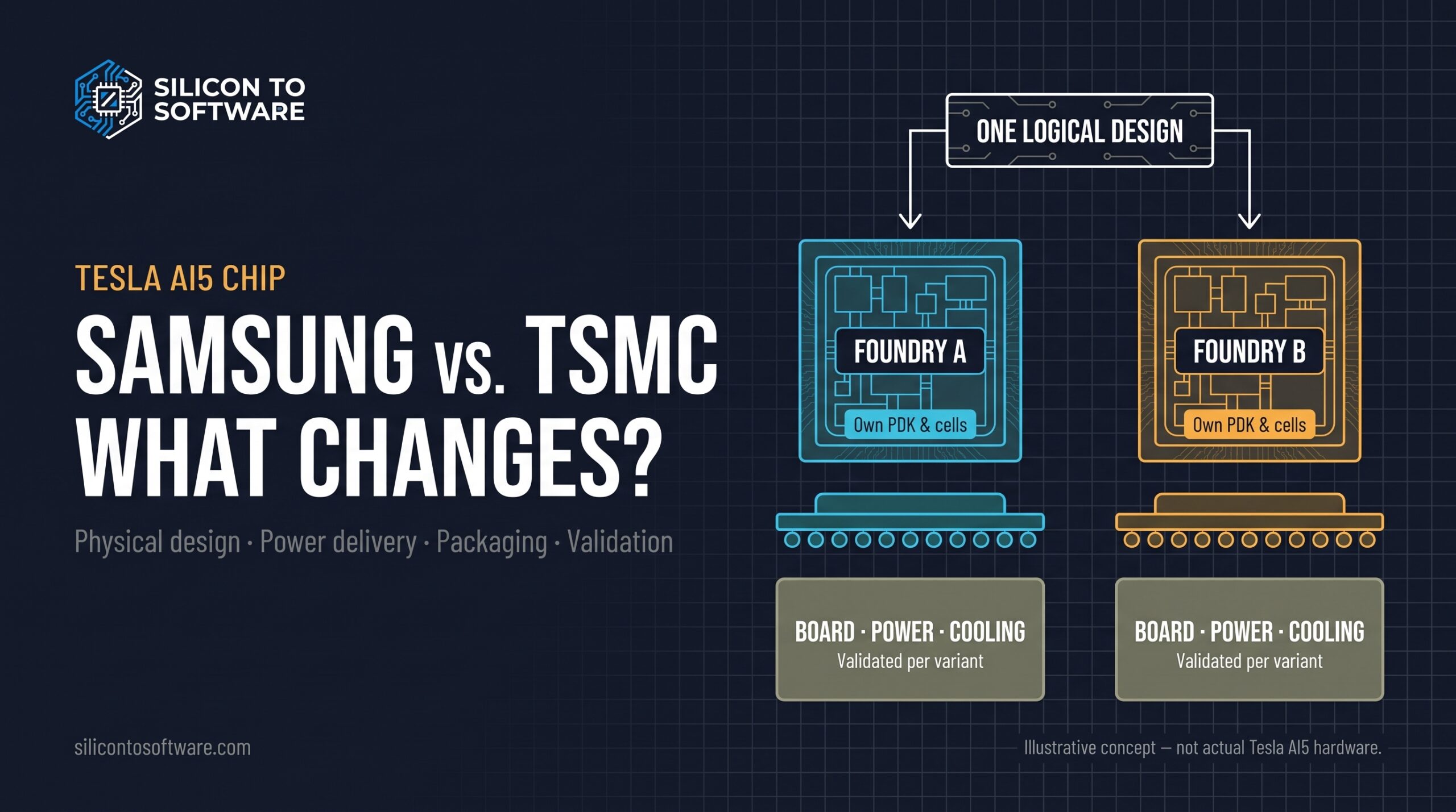
Elon Musk has said two things about Tesla’s AI5 chip that sound contradictory. Writing on X, he said the versions made at TSMC and Samsung will be slightly different because each foundry translates designs into physical form differently. Yet the goal, he said, is for Tesla’s AI software to work identically on both.
Both statements can be true because they describe different layers. The physical implementations are expected to differ. The contract they present to software is meant to stay the same.
That gap is what dual-sourcing the Tesla AI5 chip actually involves. I’ve spent more than 20 years in PCB manufacturing and technical sales, and this article gives particular attention to the part of the problem closest to that work: the package, the board, power delivery, and system qualification.
It covers three questions:
- What moves between foundries, and what has to be rebuilt?
- What can “identical” realistically mean?
- Why are the package, the PCB power delivery network (PDN), and system qualification where two chip variants either converge or don’t?
Tesla AI5 Status: What Tesla Has Said and What Is Reported
| Item | What is on record | Status |
|---|---|---|
| Production timing | Tesla’s Q4 2025 shareholder update plans AI5 production for 2027 | Company-stated |
| Design completion | Tesla’s Q1 2026 shareholder update says the final AI5 chip design was completed in April | Company-stated |
| Q2 2026 shareholder update | No AI5-specific guidance | Company document |
| Volume timing and first use | On the July 2026 earnings call, Musk said he hoped for volume production around mid-2027, initially for Optimus | Executive statement |
| Two foundries | Musk has said AI5 will be built by both Samsung and TSMC, with the versions slightly different | Executive statement |
| Samsung tape-out, process and site | A Samsung Foundry official’s LinkedIn post, as reported, cites tape-out and production on 2nm in TTexas | Reported |
| TSMC process and fab | Reported as N3E (The Bell); fab reporting cites Taiwan and Arizona | Reported, unconfirmed |
| Memory | Supplier and configuration | Unconfirmed |
| Volume split | Allocation between foundries and sites | Not disclosed |
Sources: Tesla shareholder updates and earnings-call transcripts; secondary reports as cited in Sources.
Company-stated
Design completion. Tesla’s Q1 2026 shareholder update says it completed the final chip design of its next-generation AI5 inference processor in April. On the earnings call, Musk congratulated the chip team for taping out AI5. Neither statement establishes fabricated, valid,ated or volume-production silicon.
Production plan. Tesla’s Q4 2025 update said AI5 production was planned for 2027. On the Q2 2026 call in July, Musk said he hoped AI5 would be in volume production around the middle of 2027. That is guidance, not a confirmed ramp. Tesla’s Q2 2026 update deck contains no AI5-specific guidance.
Initial deployment. On the Q1 2026 call in April, Musk said he expected AI5 to go first into Optimus and the data center. His stated rationale was that AI4 looked sufficient for unsupervised driving. He left room for vehicle use later. On the Q2 call, he said AI5 would initially go into Optimus. Tesla’s stated priorities have shifted before.
Performance target. Tesla’s Q4 2025 update says it is targeting a 50x improvement in performance for AI5 relative to AI4. Tesla credits that to three separate figures:
- 10x raw compute
- 9x memory capacity
- 5x from hardened block quantization and softmax functions
These are Tesla-reported figures, and they measure different things. Tesla has not published how they relate to the 50x figure, or the workload, precision, power condition, or benchmark method behind it. It is a target, not demonstrated performance.
Executive statements and reports
Musk on both foundries. Musk has described AI5 as being produced by Samsung and TSMC. In April 2026, he thanked both companies on X for supporting AI5 production. These are executive statements, not a published production allocation.
Samsung milestone. Yonhap News, as relayed by TrendForce, reported that a Samsung Foundry official posted on LinkedIn that AI5 had completed tape-out and was expected to enter production on Samsung’s 2nm process in Texas. Tape-out, process node, and site are three separate reported claims here. None of them is a corporate production confirmation.
Unresolved
TSMC node and fab. Korea’s The Bell reported that TSMC would use its 3nm N3E process. Other reports differ. Reporting has cited TSMC fabs in both Taiwan and Arizona. Neither Tesla nor TSMC has confirmed the node or fab.
Memory. Reports cited by TrendForce identify SK hynix in connection with AI5 memory, and separately describe Samsung LPDDR5X. The available reporting does not establish the final memory configuration, the supplier allocation, or whether these claims refer to the same implementation.
Production allocation. Tesla has not published how AI5 volume will be divided between foundries or sites.
The Tesla and Samsung tape-out statements are consistent with separate design-side and foundry-side work. They don’t establish the scope of either milestone, or how design responsibilities are divided among Tesla, Samsung,g and TSMC.
Why Tesla Is Dual-Sourcing AI5
Three distinct benefits often get blurred together:
- Supply resilience. A qualified second source is contingency capacity if one line stalls. It has value even if most volume runs through one foundry.
- Manufacturing diversification. Actual production on two processes, potentially in multiple locations. Samsung’s Texas facility and TSMC’s Arizona and Taiwan fabs have been named in executive statements and reporting. Tesla has not published how AI5 production will be allocated among them.
- Negotiating leverage. A possible commercial benefit of a second qualified source. Tesla has not stated it as a motive.
The cost of any of these is broader than a second layout. It typically includes:
- process-specific physical design
- duplicated or adapted IP
- design verification
- test development and characterization
- masks and other non-recurring engineering
- yield learning
- packaging work
- qualification for a second implementation
What Moves Between Foundries in a Chip Design, and What Doesn’t
A chip design is a stack of representations, and only part of it is foundry-neutral.
Largely reusable:
- architecture and instruction-level behavior
- RTL, the logical hardware description
- verification environments
- some soft IP delivered as RTL
Potentially reusable, with variant-specific adaptation and validation:
- firmware, drivers, compiler and software stack. Source code can carry over, but boot flows, fuse settings, memory initialization and workarounds for silicon errata may differ per variant.
Typically process-specific:
- the process design kit (PDK): device models, design rules and extraction decks
- standard-cell libraries
- SRAM compilers and memory macros, even when the logical memory interface is shared
- the metal stack
- signoff corners
- hard IP such as memory PHYs, PLLs and I/O, implemented per process even when one vendor supplies both versions
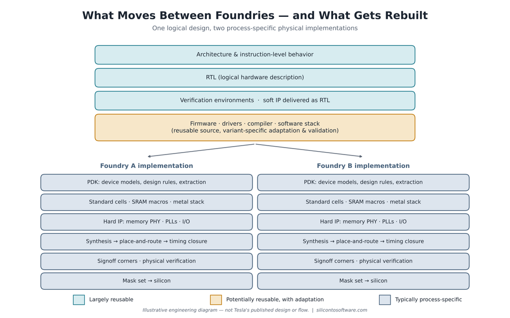
Implementing one design on two processes would therefore be expected to require substantial process-specific work for each one: synthesis, place-and-route, timing closure, physical verification and mask generation. That is the general engineering consequence. Tesla hasn’t published how that work is divided between its own team and each foundry.
Dual-sourcing one design has precedent. Apple’s 2015 A9 processor was built on Samsung’s 14nm and TSMC’s 16nm processes. That was a much smaller mobile chip on two FinFET processes, though, so it doesn’t indicate how the approach scales to a large AI accelerator or across transistor architectures.
FinFET vs. Gate-All-Around: If the Transistors Differ
Samsung introduced gate-all-around (GAA) nanosheet transistors, which it calls MBCFET, with its 3nm process, and describes its 2nm node as GAA-based as well. TSMC’s N3 family is built on fin-based (FinFET) transistors, and TSMC says its N2 uses nanosheet transistors, a gate-all-around structure. These are descriptions of each foundry’s process families. They do not establish which process AI5 uses.
- If the TSMC variant is on an N3-family node, as The Bell reported, one logical design would span two transistor architectures.
- If it is on N2, both would be GAA nanosheet processes, but different implementations with different device characteristics.
Until TSMC’s node is confirmed, this stays conditional.
Timing Closure, Power and Operating Points Across Two Processes
The same logic typically closes timing differently on two processes. Drive strength, leakage, and wire RC all differ, so critical paths and voltage-frequency curves shift.
Two conceptual endpoints frame the design choice:
- Common spec. One frequency, one power envelope, one external behavior. If both variants must meet the same performance bin or operating point, the weaker implementation sets that ceiling.
- Best-of-each. Each variant runs at its own optimum. Software and system design carry the difference.
Most real programs sit between the two. A common software interface can coexist with variant-specific clocks, voltage tables, power-management policies, performance bins, and workload scheduling. External specifications can be matched within defined limits while internal behavior differs. Those specifications include supply ranges, maximum current, power envelope,e and interface timing.
Matching the functional specification doesn’t make two variants perform identically. They can still differ in:
- performance per watt and leakage at operating temperature
- voltage and frequency guardbands and bin distribution
- maximum sustainable frequency under thermal limits
- memory-subsystem behavior
- production-test screening
Nominal performance, guaranteed worst-case performance, and sustained system performance are different measures, and they shouldn’t be treated as interchangeable. This is an engineering inference from semiconductor practice, not a characterization of AI5. Tesla hasn’t said where AI5 sits. Per-variant firmware tables behind a common interface would be one plausible approach, but that is an inference, not a published fact.
Some data-center inference and robotics workloads can impose prolonged or highly variable computational loads, unlike typical smartphone workloads. That makes sustained performance, transient power behavior, and thermal management important when qualifying different silicon implementations.
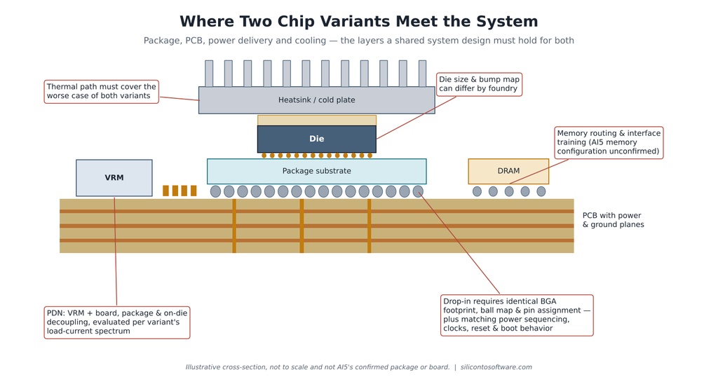
Package, PCB and Power Integrity: Where Two Chip Variants Meet the System
The package and the PCB introduce a separate set of engineering constraints.
Tesla hasn’t said whether both variants must fit the same package, board,d and cooling solution. There are two broad options:
- Common system design. Either variant can be installed in any qualified system that meets shared electrical, mechanical, firmware, and thermal requirements. This maximizes supply flexibility, but the system must tolerate both.
- Segregated or variant-specific systems. Each variant goes into its own systems. Each design is simpler, but some resilience is given back.
Tesla’s system design must address which of these applies. What follows are engineering questions for the first option, not confirmed AI5 details.
Package Pinout and Ball-Map Compatibility
Physical drop-in compatibility requires an identical BGA footprint, ball map, and pin assignment. Beneath that, the die bump map and substrate routing can differ if die sizes differ. That can change reflow warpage and solder-joint reliability, even when the board footprint matches.
Physical compatibility is necessary but not sufficient for functional interchangeability. These also have to meet common requirements:
- power sequencing and voltage tolerances
- reference clocks and reset timing
- interface training and boot behavior
- signal integrity
If Tesla doesn’t require drop-in compatibility, none of this must match.
PDN Target Impedance and Transient Current
PDN design usually starts from a first-order target impedance: allowable voltage deviation divided by worst-case transient current. That number is a budgeting tool, not a complete power-integrity criterion. Real supply behavior also depends on:
- the transient’s waveform and edge rate
- frequency-dependent impedance from the VRM through the board, package and die
- VRM control-loop response
- how the total voltage tolerance is split between regulation, ripple and droop
- whether repetitive load patterns excite resonant peaks above the target line
Two variants can stress one board differently. Different leakage changes static current, and different switching activity changes transient current.
Different on-die capacitance and package parasitics can also shift the die–package resonance. At sufficiently high frequencies, package inductance limits how effective board-level decoupling can be, so on-package and on-die solutions become increasingly important. At lower frequencies, the PCB decoupling network and the VRM have greater influence.
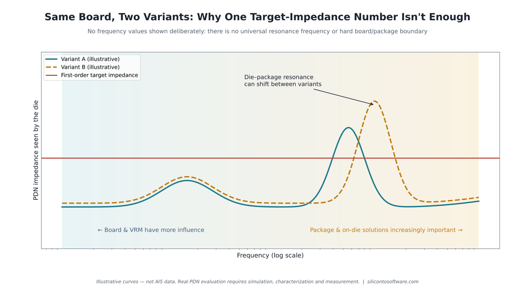
The full PDN has to be evaluated against each variant’s load-current spectrum and voltage-tolerance requirements. That evaluation should include antiresonances, where impedance is observed or measured, and coupling between power rails. These are engineering inferences, and they require simulation, characterization, and measurement to confirm.
The board-level responses each cost something:
- design for the union of both variants’ requirements
- vary the decoupling population per variant
- set VRM voltage or load-line behavior per variant in firmware
Thermal Design: Total Power, Power Density and Transients
Junction temperature depends on several factors together:
- total power dissipation
- its spatial distribution across the die
- thermal resistance and impedance from die to coolant
- cooling conditions
- how workload transients drive power over time
Two variants with similar total power can differ in hotspot distribution and transient behavior. A shared cooling solution has to cover the worse case on each of those dimensions, and firmware thermal limits may need to be set per variant.
LPDDR5X vs. HBM: An Architectural Illustration
If AI5 uses LPDDR5X, as one report states, its memory subsystem would differ structurally from the HBM-based accelerators that dominate AI coverage. The comparison below illustrates that architectural difference. It does not describe confirmed AI5 hardware.
- HBM stacks DRAM dies vertically and connects them to the processor through a very wide interface. That requires advanced packaging, typically a silicon interposer or another high-density interconnect such as embedded bridges.
- LPDDR5X, defined under JEDEC’s JESD209-5C, uses conventional DRAM packages with narrower per-device channels at high per-pin data rates. Depending on the system, it can be placed in-package on the substrate or routed across the PCB. Interface training centers its timing. Training procedures are implementation-dependent and differ across DRAM architectures.
The two differ in channel organization, routing topology, physical integration, and signal-integrity constraints.
| LPDDR5X-style memory | HBM-style memory | |
|---|---|---|
| Physical arrangement | Conventional DRAM packages, placed in-package on the substrate or routed across the PCB | DRAM dies stacked vertically beside the processor |
| Interface | Narrower per-device channels at high per-pin data rates | Very wide interface |
| Packaging | Standard package or board routing | Advanced packaging, typically a silicon interposer or embedded bridges |
| What requires revalidation | PHY integration, signal integrity, timing margins and training behavior, as applicable | PHY integration, package/interposer interfaces, signal integrity and thermal behavior, as applicable |
| Relevance to AI5 | Illustrative only. AI5 memory configuration is unconfirmed | Illustrative only. Common in data-center accelerators |
Architectural illustration only. Tesla has not confirmed AI5’s actual memory configuration or supplier.
The memory PHY is hard IP, implemented per process. If the two PHY implementations, or the DRAM parts paired with them, differ, timing margins and training behavior may differ too. A shared board would need to hold margin for both.
System Qualification Across Silicon Variants
Qualification evidence comes in distinct layers.
Component qualification. Each foundry implementation would be expected to need its own qualification baseline. JEDEC’s JESD47 (latest revision listed as JESD47N, August 2026) describes baseline stress tests for qualifying new products, product families, and products whose process is being changed. Which tests apply depends on the qualification plan, the process difference,s and the intended operating conditions.
Package qualification. If package construction differs between variants, package-level reliability evidence would differ too.
Board and system qualification. Board-level solder-joint reliability testing and system-level validation cover the configurations that ship. Evidence may be shared across configurations where similarity, change analysis and risk assessment justify it.
Automotive qualification. Requirements, including AEC-Q100 where applicable, depend on the intended application, device classificati, on and customer requirements.
This is where a dual-foundry hedge gets paid for: in validation hours and system margin.
What “Works Identically” Means for AI5 Software
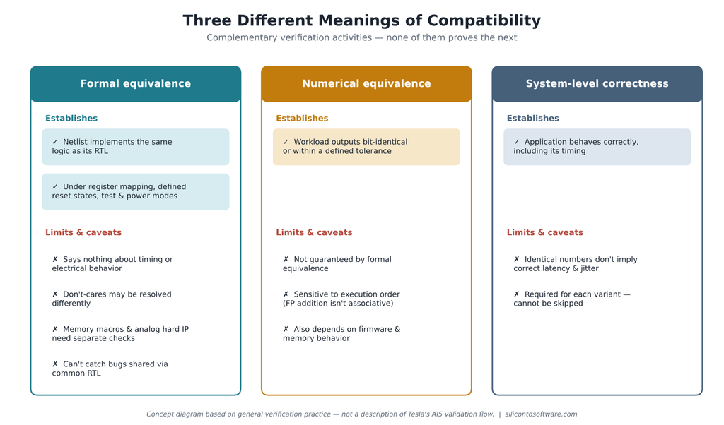
“Identical” can mean three different things. They are complementary verification activities, and none of them proves the next.
1. Formal equivalence
Logic equivalence checking can show that a netlist implements the same logic as its RTL. That result depends on register mapping, defined reset states, and constraints such as test and power modes. It can be applied before and after physical implementation.
It has limits:
- Sequential optimizations may require separate sequential-equivalence methods.
- RTL don’t-care conditions can be resolved differently in each implementation.
- Memory macros and analog hard IP such as PHYs and PLLs are verified by other means.
- Both variants inherit any bug in the shared RTL.
- It says nothing about timing or electrical behavior. Those are established through static timing analysis, parasitic extraction, signal-integrity signoff and silicon characterization across process, voltage and temperature corners.
Formal equivalence is a foundation for software compatibility, not proof of it.
2. Numerical equivalence
Numerical equivalence means outputs from complete workloads are bit-identical, or fall within a defined tolerance. Formal equivalence doesn’t guarantee it. Whole-workload results also depend on execution ordering, numerical formats, firmware, memory behavior, nondeterministic operations, and implementation-defined behavior.
Floating-point addition isn’t associative, so a different reduction order can change low-order bits even on one chip. Different implementations of an operation can still produce the same results, provided the operation’s rounding and accumulation behavior is fully specified. That matters especially for low-precision formats.
3. System-level correctness
The application behaves correctly, including its timing. A robot control loop cares about latency and jitter, not just the numbers. Two variants producing identical outputs at different speeds can still behave differently as systems. That is an engineering inference, and it’s why system-level validation on both variants can’t be skipped.
Tesla hasn’t said which of these it targets, or how.
Yield and Cost: Why the Two Lines May Not Ramp Alike
Processes at different maturity levels ramp differently. Defect density, parametric yield, and cost per good die can diverge. I’m excluding yield and cost figures because the numbers in circulation are anonymously sourced.
A faster ramp doesn’t automatically make one foundry the principal source. Capacity contracts, qualification status, and commercial allocation also decide where volume goes. If volume does concentrate on one line, the second implementation provides contingency value rather than parallel supply. That is less than full diversification, but still worth something.
What to Watch Next for Tesla AI5
- Engineering samples from both foundries, and any statement about matching them to a common spec.
- Confirmation of TSMC’s node and fab.
- Whether variants share systems or are deployed separately.
- How volume splits once high-volume manufacturing begins.
- Whether AI5 returns to the vehicle roadmap.
Conclusion: The Price of a Foundry-Portable AI Chip
Dual-sourcing AI5 is a hedge paid for in engineering effort. The bill covers process-specific implementation work and validation repeated at every variant-dependent layer. If the variants share systems, it also covers a power and thermal envelope wide enough for both.
The open test is whether two physical chips can hold one software contract at Optimus and data-center volume. Tesla’s system design must also address whether they share one system envelope, or whether their differences are handled with variant-specific systems.
If Tesla manages it, AI5 will show that this design, under this implementation strategy, could be built at two foundries and behave as one product. That is narrower than proving leading-edge AI accelerators are generally foundry-portable, but it would still be meaningful. If one line quietly becomes primary, the industry learns what that portability costs.
About the Author
Imran Valiani | Sales Director, PCB Electronics Manufacturing
20+ years working with major Bay Area and global tech clients. Founder of Silicon to Software, where I write about the hardware layer — PCB fab, AI gear, autonomous systems, and cyber — the stuff most tech writers have never touched. Literally.
Follow: X @SiToSoftware | LinkedIn
For more analysis of chip scaling, advanced packaging, memory, and semiconductor engineering constraints, explore the Semiconductor Engineering & Advanced Packaging Resource Hub.
This article was developed with AI assistance and edited, fact-checked, and reviewed by the author. See my full AI disclosure.
Sources
Tesla — primary company documents
- Tesla — “Q4 and FY 2025 Update” (Exhibit 99.1, Form 8-K), U.S. Securities and Exchange Commission, January 28, 2026. Primary. https://www.sec.gov/Archives/edgar/data/1318605/000162828026003837/exhibit991.htm
- Tesla — “First Quarter 2026 Update” (Form 8-K), Tesla Investor Relations, April 22, 2026. Primary. https://ir.tesla.com/_flysystem/s3/sec/000162828026026551/tsla-20260422-gen.pdf
- Tesla — “Q2 2026 Update” (Exhibit 99.1, Form 8-K), U.S. Securities and Exchange Commission, July 22, 2026. Primary. Contains no AI5-specific guidance. https://sec.gov/Archives/edgar/data/1318605/000162828026049213/exhibit991.htm
Tesla — earnings call transcripts (third-party)
- MarketBeat — “Tesla Q1 2026 Earnings Call Transcript” MarketBeat, April 2026. Third-party transcript. https://www.marketbeat.com/earnings/reports/2026-4-22-tesla-inc-stock/
- 24/7 Wall St. — Tesla Q1 2026 earnings live coverage 24/7 Wall St., April 22, 2026. Third-party relay of call remarks. https://247wallst.com/investing/2026/04/22/live-will-tesla-soar-after-announcing-q1-earnings/liveupdates/10/
- Investing.com — “Earnings call transcript: Tesla Q2 2026 revenue beats, EPS misses as stock falls” Investing.com, July 2026. Third-party transcript. Supports the mid-2027 / Optimus-first remarks. https://www.investing.com/news/transcripts/earnings-call-transcript-tesla-q2-2026-revenue-beats-eps-misses-as-stock-falls-93CH-4807216
Executive statements and AI5 reporting (secondary)
- Drive Tesla Canada — “Elon Musk Reveals Tesla AI Chip Production Timelines Through 2028” Drive Tesla Canada, November 2025. Secondary report of Musk’s X post. https://driveteslacanada.ca/news/elon-musk-reveals-tesla-ai-chip-production-timelines-through-2028/
- Korea Economic Daily — Musk’s April 15, 2026 AI5 tape-out post (Japanese edition), Korea Economic Daily via Bloomingbit, April 2026. Secondary report of Musk’s X post. https://jp.bloomingbit.io/feed/news/110064
- TrendForce — “[News] Samsung Reportedly Completes Tesla AI5 Tape-out, Paving the Way for 2nm Ramp at Taylor Fab” TrendForce, July 13, 2026. Secondary; relays Yonhap News. https://www.trendforce.com/news/?p=60735
- TrendForce — “[News] Musk Signals Tesla AI5 Mass Production Delay to 2027, Casting Uncertainty Over Samsung” TrendForce, 2025. Secondary; relays The Bell’s N3E report. https://www.trendforce.com/news/?p=47831
- TrendForce — “[News] Tesla AI5 Reportedly Uses SK hynix Memory, Samsung LPDDR5X; Samsung SF2T Process Applied Ahead of AI6” TrendForce, April 16, 2026. Secondary; relays Hankyung and Newsis. https://www.trendforce.com/news/2026/04/16/news-tesla-ai5-reportedly-uses-sk-hynix-memory-samsung-lpddr5x-samsung-sf2t-process-applied-ahead-of-ai6/
Foundry process technology
- Samsung Electronics — “Samsung Begins Chip Production Using 3nm Process Technology With GAA Architecture” Samsung Global Newsroom, June 30, 2022. Primary. https://news.samsung.com/global/samsung-begins-chip-production-using-3nm-process-technology-with-gaa-architecture
- Samsung Foundry — “Process Technology – Logic Node” Samsung Semiconductor, page updated August 2026. Primary. Lists GAA among its 12-inch technologies and states that SF2 started mass production in 2025. The node-by-node architecture detail is not machine-readable on this page. https://semiconductor.samsung.com/foundry/process-technology/logic-node/
- Korea JoongAng Daily — “Samsung unveils Exynos 2600 mobile chip slated to power Galaxy S26 series” Korea JoongAng Daily, December 2025. Secondary; relays Samsung’s official disclosure that its 2nm node is GAA-based. https://www.koreajoongangdaily.com/business/samsung-unveils-exynos-2600-mobile-chip-slated-to-power-galaxy-s26-series/11989445
- TSMC — “TSMC FINFLEX™, N2 Process Innovations Debut at 2022 North American Technology Symposium” TSMC Press Center, June 16, 2022. Primary. Covers N3/N3E fin-based FINFLEX cells and the N2 nanosheet transistor architecture. https://pr.tsmc.com/english/news/2939
Historical precedent (secondary)
- Phone Scoop — “Apple: A9-Driven Battery Variances Limited to 2-3%” Phone Scoop, October 9, 2015. Secondary. Documents the A9’s dual sourcing on Samsung 14nm and TSMC 16nm. https://www.phonescoop.com/articles/article.php?a=16602
Standards
- JEDEC — “Stress Test Driven Qualification of Integrated Circuits” (JESD47N), JEDEC Solid State Technology Association, August 2026. Standards body; product listing verified on jedec.org. https://www.jedec.org/https%3A//jedec.dpdcart.com/cart/add%3Fproduct_id%3D250982%26method_id%3D274100
- JEDEC — “Low Power Double Data Rate (LPDDR) 5/5X” (JESD209-5C) JEDEC Solid State Technology Association, July 2023. Standards body; verified on jedec.org. https://www.jedec.org/node/9058
Engineering references
- Larry Smith, Steve Sandler and Eric Bogatin — “Target Impedance Is Not Enough” Signal Integrity Journal. Industry technical article. Covers target impedance as a standard PDN tool and its limitations. The link goes to the author’s article listing, where this article appears. https://www.signalintegrityjournal.com/authors/213-larry-smith/articles
- Jingook Kim et al. — “Closed-Form Expressions for the Maximum Transient Noise Voltage Caused by an IC Switching Current on a Power Distribution Network” IEEE Transactions on Electromagnetic Compatibility, vol. 54, no. 5, pp. 1112–1124. Peer-reviewed; institutional repository record. https://scholarworks.unist.ac.kr/handle/201301/3074?mode=full
- Indian Institute of Science — “Antiresonance and Noise Suppression Techniques for Digital Power Distribution Networks” IISc electronic theses repository. Academic thesis. Covers the target-impedance definition, its flat-impedance assumption, and PDN antiresonance. https://etd.iisc.ac.in/handle/2005/3967
- D. J. Greaves — “Boolean Equivalence Checker” (System-on-Chip Design lecture notes), University of Cambridge Computer Laboratory. Academic course material. Covers RTL-to-netlist equivalence, post-place-and-route netlist checks, and don’t-care conditions. https://www.cl.cam.ac.uk/teaching/1516/SysOnChip/sp5-abd/zhpf4497915e.html
- David Goldberg — “What Every Computer Scientist Should Know About Floating-Point Arithmetic” ACM Computing Surveys, March 1991; reprinted in Oracle’s Numerical Computation Guide. Peer-reviewed. Covers order-dependent floating-point sums and the bit-identical results of exactly rounded IEEE operations. https://docs.oracle.com/cd/E19957-01/806-3568/ncg_goldberg.html