MicroLED vs OLED vs LCD: Why MicroLED Is So Hard to Manufacture
MicroLED promises OLED-level contrast, higher brightness, and long display life. But transferring millions of microscopic LEDs with high yield remains one of the hardest problems in display manufacturing.
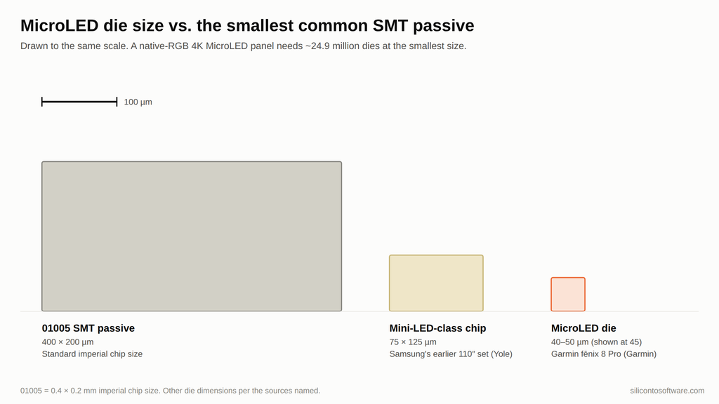
A 4K display has 8,294,400 pixels. In a native-RGB MicroLED panel, each pixel uses separate red, green, and blue emitters. That makes 24,883,200 microscopic LEDs, and each one has to be grown, transferred, bonded, and proven to work.
Yield is what turns that number into a manufacturing problem:
| Subpixel yield | Dead subpixels on one 4K panel, before repair |
|---|---|
| 99.99% | ~2,488 |
| 99.999% | ~249 |
| 99.9999% | ~25 |
99.99% sounds exceptional until it’s multiplied across nearly 25 million emitters: it leaves roughly 2,500 dead subpixels, and six nines still leaves about 25. At that scale, raw transfer yield alone isn’t enough. Commercial MicroLED manufacturing depends on inspection, redundancy, repair, or some combination of them, covered below.
That arithmetic is the real answer to the MicroLED vs OLED vs LCD question. On paper, MicroLED combines some of the strongest attributes of OLED and inorganic LEDs. The problem is turning those advantages into manufacturable displays at competitive yield and cost, and some of that difficulty is device physics, not just the factory.
MicroLED products do exist, and their prices make the point:
- Garmin Fenix 8 Pro MicroLED, which Garmin describes as the first smartwatch with a MicroLED display, launched in September 2025 at $1,999.99. Its list price was cut to $1,699.99 in February 2026.
- Samsung’s 114-inch MicroLED TV launched in the US in 2024 at $149,999.99. As of September 2026, Samsung Canada listed it as out of stock.
What doesn’t exist is MicroLED in a mainstream phone, laptop, or living-room TV. This article explains what separates the three technologies, where MicroLED manufacturing breaks down, and why the first products were watches and walls. It’s written from the PCB and electronics manufacturing side, where yield, placement, and cost per good unit decide what ships.
Key takeaways
- Mini-LED and “Micro RGB” TVs are LCDs. Only MicroLED makes light directly from inorganic LEDs at the pixel level.
- A 4K MicroLED panel needs ~24.9 million working LEDs, so even six-nines yield requires repair.
- Epitaxy, die shrink, mass transfer, and repair each add yield loss and cost.
- ams OSRAM’s cancellation, the reported Apple exit, and Samsung’s reported pullback all point to the same pressure: manufacturing economics and process complexity.
Table of Contents
MicroLED vs OLED vs LCD: How Each Display Makes Light
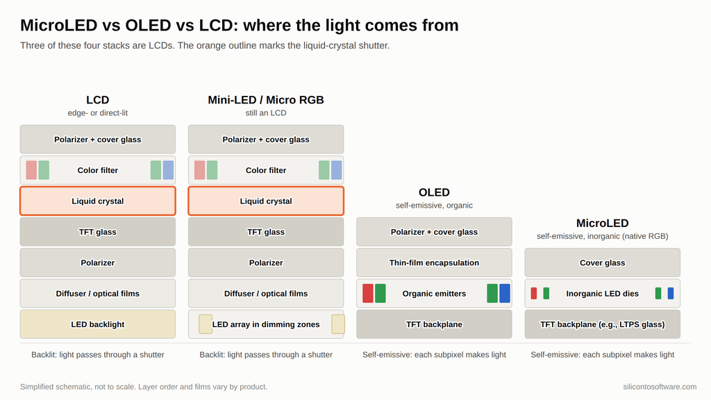
LCD, Mini-LED, and Micro RGB: three backlights, one shutter
An LCD doesn’t emit light. A backlight shines through a liquid-crystal layer that acts as a per-pixel shutter, and color filters or quantum-dot layers produce red, green, and blue. The liquid crystal never blocks all of the light, and that sets the black level.
Mini-LED divides the backlight into thousands of small LEDs grouped into local-dimming zones. Each zone is still larger than a pixel, so wherever bright and dark areas meet, light spills into the dark side. That spillover is the halo, or blooming, effect. More zones shrink the halo, but it can’t reach zero until every pixel is its own light source.
Micro RGB is Samsung’s 2026 flagship. Samsung describes it as a micro-sized RGB color backlight, and VDE has certified the LEDs at ≤100 µm. Independent coverage confirms it is an RGB LED backlight behind an LCD panel. A 55-inch Micro RGB TV that launched at $1,599.99 is an LCD, not a MicroLED display.
Rule of thumb: if there’s a liquid-crystal layer, it’s an LCD, no matter what the backlight LEDs are called.
OLED: every pixel emits, and every pixel ages
OLED removes the backlight. Each subpixel is an organic emitter that makes its own light and can switch fully off, which gives true black.
Organic emitters degrade permanently. Burn-in happens because pixels showing different content for different durations degrade unevenly. The three colors also age at different rates, so color balance drifts over the display’s life. Manufacturers manage this with pixel shifting, compensation algorithms, and brightness limiting. My interpretation is that those limits are part of why OLED has historically traded peak brightness for lifetime.
MicroLED: self-emissive, inorganic
In native-RGB MicroLED, each subpixel is an inorganic III-V semiconductor emitter: InGaN for blue and green, and typically AlGaInP for red. Other architectures use blue or UV MicroLEDs with color-conversion layers, covered below.
That supports higher brightness and far lower burn-in risk. Garmin’s company-stated position is that inorganic LEDs can be damaged by overheating but don’t wear out through normal use. The accurate claim is lower risk, not immunity.
| LCD / Mini-LED / Micro RGB | OLED | MicroLED | |
|---|---|---|---|
| Light source | Backlight + LC shutter | Self-emissive, organic | Self-emissive, inorganic |
| Per-pixel black | No (zone-limited) | Yes | Yes |
| Burn-in risk | Not from differential emitter aging | Yes (differential aging) | Much lower (inorganic; company-stated) |
| Mainstream availability (2026) | Yes | Yes | No |
MicroLED Manufacturing: Why It’s So Hard to Scale
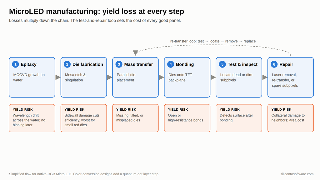
OLED emitters are deposited directly onto the backplane. MicroLED emitters are grown on a separate wafer, singulated into millions of discrete dies, and physically moved. Every step has its own yield loss.
Epitaxy: wavelength uniformity has to be built in
MicroLED color is set during MOCVD growth. InGaN emission wavelength depends on indium composition, which depends on growth temperature and gas flow. A 1 °C difference in growth temperature shifts the wavelength by 1.8 nm for blue LEDs and 2.5 nm for green.
Conventional LEDs absorb that variation by sorting and binning finished parts. MicroLEDs can’t be sorted and binned the way conventional LEDs are, so the epitaxial growth itself has to carry most of the uniformity burden. Industry work published during the early commercialization push (2018–2019) cited MicroLED epiwafer targets of roughly ±1 nm to ±4 nm, depending on application and transfer approach, compared with around 8–10 nm for conventional LED epitaxy. Treat those as historical industry targets rather than a current universal specification. The direction hasn’t changed.
Any variation the reactor doesn’t control has to be corrected in the drive electronics, and that correction has its own cost.
Die size and red efficiency: cheaper dies, dimmer dies
Smaller dies mean more LEDs per wafer and lower cost. But peer-reviewed studies show red micro-LED external quantum efficiency (EQE) drops sharply as die size shrinks, because of non-radiative recombination at sidewall defects.
The mechanism:
- Mesa etching leaves damaged sidewalls.
- Smaller dies have proportionally more sidewall.
- Red AlGaInP has a longer minority carrier diffusion length than GaN, so more carriers reach those sidewalls and recombine without emitting light.
Laboratory sidewall treatments narrow the gap. A 2023 Applied Physics Express study of treated AlGaInP devices reported only a 20% EQE reduction when shrinking from 100 × 100 µm to 20 × 20 µm. Whether that holds at production volume is a separate question.
Some approaches avoid native red emitters altogether. Quantum-dot color conversion, typically paired with blue or UV micro-LEDs, is one of the main full-color routes. It removes the red-emitter problem but adds a conversion layer to the stack.
MicroLED mass transfer: why pick-and-place doesn’t scale
Anyone who has run an SMT line can do this arithmetic. At an illustrative 100,000 placements per hour, 24.9 million placements take about 249 hours. That’s more than ten days for one 4K panel, before test or repair.
No one builds MicroLED panels this way. The arithmetic shows why they can’t. Serial pick-and-place belongs to coarse-pitch LED boards and backlights; fine-pitch MicroLED needs a fundamentally parallel process.
Mass transfer moves large arrays of dies to the backplane in each operation. Published methods include laser-based, electrostatic, fluidic self-assembly, elastomer stamp, and roll-to-roll transfer. A 2024 APL Materials paper summarizes the trade-offs:
- Electrostatic: precise, but costly and can damage chips.
- Stamp: cheap, but inefficient for large, dense arrays.
- Fluidic self-assembly: historically hard to control, poorly selective, and low-yield.
Those characterizations aren’t permanent. A 2023 Nature paper from Seoul National University and LG researchers assembled more than 19,000 disk-shaped 45 µm GaN chiplets in 60 seconds at 99.88% yield, using a viscosity-controlled fluid. That’s a laboratory demonstration, not 4K RGB production, but it shows how quickly the transfer-method trade-offs are moving.
Die size matters here too. TrendForce noted that ams OSRAM’s smaller vertical chips reduced cost and helped redundancy design, but demanded tighter transfer precision, which it called another mass-production bottleneck.
Bonding and backplanes: from PCB to LTPS glass
The backplane sets the achievable pixel pitch, and this is where MicroLED’s history runs through the PCB world. According to Yole Group’s CES 2022 analysis:
- Samsung’s earlier 110-inch set was marketed as MicroLED but was built much like The Wall: passive-matrix mini-LED-class chips (75 × 125 µm) on PCB, placed by standard pick-and-place.
- Samsung’s 2022 89- and 101-inch models moved to smaller dies on 12-inch LTPS glass tiles, placed by laser-based mass transfer.
Samsung’s own product history shows the same naming problem this article started with.
My interpretation: PCB modules worked while dies were large enough for conventional placement and pitch was coarse enough for tiling. Once pitch tightened, the design moved onto glass and placement moved to parallel transfer. Both transitions happened at the same point. (Related: how chip scaling moved from the transistor to the interconnect.)
Testing and repair: the known-good-die problem
Advanced packaging already lives with this constraint in chiplets and HBM: test before you commit, because one bad die can scrap an expensive assembly. (See why HBM4’s real limit is packaging.) MicroLED faces the same problem across millions of dies.
For high-quality consumer displays, defective pixels have to be driven to extremely low levels, so manufacturers need a defect-management strategy:
- Redundancy: spare subpixels replace defective ones. This costs die area, backplane area, and drive complexity.
- Repair: defective dies are removed, often by laser, and replaced. The risk is damaging neighboring electrodes, transistors, and circuits.
The throughput of the test → locate → remove → re-transfer loop sets the cost of every good panel.
MicroLED Yield Economics: What the Industry’s Decisions Show
ams OSRAM, February 2024. On February 28, 2024, ams OSRAM disclosed that a cornerstone microLED project had been unexpectedly canceled. It estimated EUR 600–900 million in non-cash impairments and said it would review its 8-inch Kulim, Malaysia facility. The customer was not named.
TrendForce identified the program as the Apple Watch, with ams OSRAM supplying chips and LG Display handling the glass backplane and mass transfer. TrendForce estimated MicroLED panel costs at potentially 2.5–3× those of comparable OLED panels.
Newer cost data. In February 2026, UBI Research put the bill of materials for a 101-inch MicroLED TV at about $52,000, with panel materials, including pixels, accounting for 86.2%. Its analyst said improving process yield is essential.
Apple, March 2024 (reported). Analyst Ming-Chi Kuo said production costs made the product economically unviable. Bloomberg reported that Apple ended its in-house microLED screen effort. Apple owned the design and manufacturing process but relied on partners for mass production and LED transfers. Apple has not confirmed either report.
Samsung, 2026 (reported). Citing ETNews, TechRadar reported that Samsung had been selling around 100 MicroLED TVs a year, had stopped build-to-order production, and had outsourced panel manufacturing and bonding. TrendForce described a phased adjustment driven by process complexity and cost.
Taken together, these decisions point to the same commercial pressure: MicroLED’s performance advantages have not yet overcome the economics and process complexity of manufacturing it at scale. The same pattern, where manufacturing capacity rather than design decides what scales, appears in AI chip packaging.
Why Small and Huge MicroLED Screens Came First
Huge screens: tiling
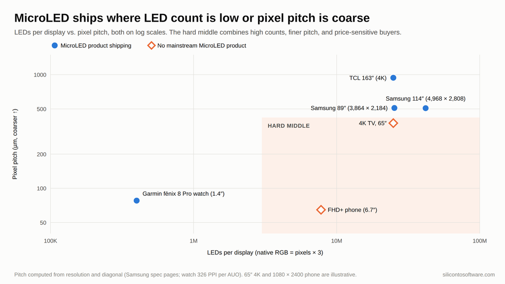
Samsung’s 2022 89- and 101-inch models used 12-inch LTPS tiles, and its commercial system, The Wall, scales to 292 inches diagonal. Each tile can be built, tested, and replaced individually, and coarse pitch allows larger dies and looser tolerances.
Prices at this end are falling but remain far from mainstream. Samsung’s 114-inch set launched at $149,999.99. TCL’s 163-inch Max163M has since launched in China at a reported 249,999 RMB, roughly £27,400.
Small screens: LED count
Garmin’s 1.4-inch, 454 × 454 panel is made by AUO. Garmin’s display technology manager, Ralph Polshak, described it as more than 400,000 discrete LEDs of 40–50 microns, which is under 2% of a 4K panel’s count. At launch, Garmin called it the brightest smartwatch screen ever made, at 4,500 nits.
That brightness lead didn’t last. In July 2026, Samsung’s Galaxy Watch Ultra2 arrived with a manufacturer-rated peak brightness of up to 5,000 nits, above Garmin’s 4,500-nit MicroLED rating. Samsung qualifies that figure as localized peak brightness under high ambient light, so this is a comparison of manufacturer ratings, not an independent panel measurement. My read: OLED closed the brightness gap faster than MicroLED closed its cost gap.
The power problem
The efficiency promise hasn’t arrived in shipping hardware yet. Garmin rates the MicroLED version at up to 10 days in smartwatch mode, against up to 27 for the AMOLED version. The MicroLED watch is also thicker, partly because touch isn’t yet integrated into the panel. Polshak said OLED has a 25-year head start, and that MicroLED power efficiency will improve, just not yet.
Peer-reviewed work points to a candidate mechanism. As micro-LEDs shrink, peak efficiency falls and moves to higher current densities, which the authors say can raise power consumption and self-heating in displays. According to patent literature, display pixels are typically driven well below the roughly 1 A/cm² where micro-LED efficacy tends to peak. The public record doesn’t establish how much of Garmin’s battery gap this explains.
Garmin’s Fenix 9 Pro then launched with a 3,000-nit AMOLED display and no MicroLED option.
The hard middle
Phones, laptops, and 55–65-inch TVs need fine pitch and high pixel counts. That’s where dies are smallest, red efficiency is weakest, transfer tolerances are tightest, and buyers are most price-sensitive.
The Metric to Watch
Emissive inorganic pixels still hold the burn-in advantage, but 2026 showed that OLED can close gaps quickly, including on brightness. The open question is whether transfer, test, and repair throughput can bring cost per good panel into the middle of the size range before improving OLEDs and RGB micro-LED backlights take that market for good. Samsung’s 2026 lineup suggests the backlight route is winning the first round.
Brightness demos will keep improving. Transfer yield, repair cycle time, and cost per good panel will decide whether MicroLED reaches mainstream devices. (More on the hardware layer in Emerging Technologies.)
About the Author
Imran Valiani | Sales Director, PCB Electronics Manufacturing
20+ years working with major Bay Area and global tech clients. Founder of Silicon to Software, where I write about the hardware layer — PCB fab, AI gear, autonomous systems, and cyber — the stuff most tech writers have never touched. Literally.
Follow: X @SiToSoftware | LinkedIn
This article was developed with AI assistance and edited, fact-checked, and reviewed by the author. See my full AI disclosure.
Sources
Company documentation
- Garmin — “Garmin announces the fenix 8 Pro smartwatch with inReach” Garmin, 2025. https://www.garmin.com/en-US/newsroom/press-release/wearables-health/introducing-fenix-8-pro-the-first-ever-smartwatches-from-garmin-with-inreach-technology-for-satellite-and-cellular-connectivity/
- AUO — “AUO and Garmin Launch First Micro LED Smartwatch” AUO, 2025. https://www.auo.com/en-global/New_Archive/detail/News_Archive_Product_20250904
- Garmin — “Garmin announces the fenix 9 and fenix 9 Pro GPS smartwatch” Garmin, 2026. https://www.garmin.com/en-US/newsroom/press-release/outdoor/garmin-expands-its-flagship-performance-smartwatch-lineup-with-fenix9-and-fenix9-pro/
- Samsung — “What is Micro RGB TV? | 4K TV Technology Guide” Samsung USA. https://www.samsung.com/us/tvs/tv-buying-guide/what-is-micro-rgb/
- Samsung — “Samsung Expands Premium Micro RGB TV Lineup for 2026 with New Sizes and Advanced Features” (VDE ≤100 µm footnote) Samsung Newsroom Australia. https://news.samsung.com/au/samsung-expands-premium-micro-rgb-tv-lineup-for-2026-with-new-sizes-and-advanced-features
- Samsung — “114 Inch Micro LED TV MS1C” (availability status) Samsung Canada. https://www.samsung.com/ca/tvs/micro-led/114-inch-micro-led-tv-mna114ms1ccxzc/
- Samsung — “Samsung Galaxy Watch Ultra2 and Watch9: Your Health Companion on the Wrist” (5,000-nit footnote) Samsung Global Newsroom, 2026. https://news.samsung.com/global/samsung-galaxy-watch-ultra2-and-watch9-your-health-companion-on-the-wrist
- ams OSRAM — “ams OSRAM revises microLED strategy after project cancellation” ams OSRAM, 2024. https://ams-osram.com/news/press-releases/revised-microled-strategy
- U.S. Patent 11,676,529 — “Methods and apparatus for in-pixel driving of micro-LEDs” USPTO https://image-ppubs.uspto.gov/dirsearch-public/print/downloadPdf/11676529
Peer-reviewed research
- J. Lei, H. Zhu, X. Huang, J. Lin, Y. Zheng, Y. Lu, Z. Chen, W. Guo — “Mini-LED Backlight: Advances and Future Perspectives” Crystals, 14(11), 922, 2024. DOI: 10.3390/cryst14110922 https://doi.org/10.3390/cryst14110922
- J. Lee — “Lifetime modeling for organic light-emitting diodes: a review and analysis” Journal of Information Display, 24(1), 57–70, 2023. DOI: 10.1080/15980316.2022.2126018 https://www.tandfonline.com/doi/full/10.1080/15980316.2022.2126018
- E. Tankelevičiūtė, I. D. W. Samuel, E. Zysman-Colman — “The Blue Problem: OLED Stability and Degradation Mechanisms” The Journal of Physical Chemistry Letters, 15(4), 1034–1047, 2024. DOI: 10.1021/acs.jpclett.3c03317 https://pubs.acs.org/doi/10.1021/acs.jpclett.3c03317
- S. Zhang et al. — “Research Progress of Micro-LED Display Technology” Crystals, 13(7), 1001, 2023. DOI: 10.3390/cryst13071001 https://www.mdpi.com/2073-4352/13/7/1001
- W. Sun, S. Ge, J. Li, L. Shen, X. Zhao, R. Shi, J. Zhang, Y. Xi — “Performance Investigation of AlGaInP Light-Emitting Diodes” Nanomaterials, 16(8), 480, 2026. DOI: 10.3390/nano16080480 https://doi.org/10.3390/nano16080480
- M. S. Wong, R. C. White, S. Gee, T. Tak, S. Gandrothula, H. Choi, S. Nakamura, J. S. Speck, S. P. DenBaars — “Recovering the efficiency of AlGaInP red micro-LEDs using sidewall treatments” Applied Physics Express, 16, 066503, 2023. DOI: 10.35848/1882-0786/acdf3c https://iopscience.iop.org/article/10.35848/1882-0786/acdf3c
- T. Xuan, S. Shi, L. Wang, H.-C. Kuo, R.-J. Xie — “Inkjet-Printed Quantum Dot Color Conversion Films for High-Resolution and Full-Color Micro Light-Emitting Diode Displays” The Journal of Physical Chemistry Letters, 11(13), 5184–5191, 2020. DOI: 10.1021/acs.jpclett.0c01451 https://pubs.acs.org/doi/10.1021/acs.jpclett.0c01451
- Y. Xie et al. — “High-yield Micro-LED laser transfer accomplished using an ablation-type release material” APL Materials, 12, 101111, 2024. https://pubs.aip.org/aip/apm/article/12/10/101111/3317310/High-yield-Micro-LED-laser-transfer-accomplished
- D. Lee et al. — “Fluidic self-assembly for MicroLED displays by controlled viscosity” Nature, 2023. DOI: 10.1038/s41586-023-06167-5 https://www.nature.com/articles/s41586-023-06167-5
- W. Jung, J. Choi, G. Jeon, N. Kim, J. An, I. Jang, S. Jeong, Y.-J. Kim, H. Keum — “Interface identification in micro-LED repair applications via depth profiling using femtosecond laser-induced breakdown spectroscopy” Scientific Reports, 15, 40897, 2025. DOI: 10.1038/s41598-025-24765-3 https://www.nature.com/articles/s41598-025-24765-3
- W. J. Baek, J. Park, J. Shim, B. H. Kim, S. Park, H. S. Kim, D.-M. Geum, S. H. Kim — “Ultra-low-current driven InGaN blue micro light-emitting diodes for electrically efficient and self-heating relaxed microdisplay” Nature Communications, 14, 1386, 2023. DOI: 10.1038/s41467-023-36773-w https://www.nature.com/articles/s41467-023-36773-w
Industry research and analysts
- TrendForce — “Micro LED Apple Watch Production Faces Significant Changes as Collaboration with ams OSRAM Ends, Says TrendForce” TrendForce, 2024. https://www.trendforce.com/presscenter/news/20240301-12054.html
- TrendForce — “[News] Samsung Electronics Rumored to Adjust Micro LED TV Manufacturing Strategy” TrendForce, 2026. https://www.trendforce.com/news/2026/05/13/news-samsung-electronics-rumored-to-adjust-micro-led-tv-manufacturing-strategy/
- UBI Research — “UBI Research Publishes ‘101-inch Micro-LED TV Set BOM Analysis Report’… Signaling a Game Changer for the Consumer Electronics Market” UBI Research, 2026. https://en.ubiresearchnet.com/101-inch-micro-led-tv-bom-cost-analysis-report/
- Eric Virey, Yole Group — “CES 2022 display review (Part 2): microLED, AR and direct view miniLED displays” Yole Group, 2022. https://www.yolegroup.com/strategy-insights/ces-2022-display-review-part-2-microled-ar-and-direct-view-miniled-displays/
- LEDinside — “Veeco and ALLOS Update Their Progress for 200mm GaN-on-Si Micro LED Production and Applications” (historical industry target) LEDinside, 2018. https://www.ledinside.com/press/2018/11/veeco_and_allos_update_their_progress_for_200mm_ganonsi_micro_led_production_and_applications
- LEDinside — “Epitaxy Wafer: The Fundamental Phase for Micro LED Display” (historical industry figure) LEDinside, 2019. https://www.ledinside.com/news/2019/5/epitaxy_wafer_the_fundamental_phase_microled_display
- Mini/Micro LED — “Micro LED For Waveguides: Full-Color AR Nears Production” (color-conversion routes) minimicroled.com, 2025. https://www.minimicroled.com/micro-led-for-waveguides-full-color-ar-nears-mass-production/
Reporting and interviews
- Mark Gurman — “Apple Scraps Plan to Design Display for Watch In-House, Cuts Jobs” Bloomberg, 2024. https://www.bloomberg.com/news/articles/2024-03-22/apple-scraps-plan-to-design-display-for-watch-in-house-cuts-jobs
- MacRumors — “Kuo: Apple Watch Ultra With MicroLED Display Indeed Canceled” MacRumors, 2024. https://www.macrumors.com/2024/03/01/kuo-says-microled-apple-watch-ultra-canceled/
- ETNews — “삼성전자, ‘100대 남짓’ 마이크로 LED TV 사업 축소 수순” (Samsung Electronics moves to scale back its ~100-unit Micro LED TV business) ETNews, 2026. https://www.etnews.com/20260504000265
- TechRadar — “Are micro-LED TVs cooked? A new report says Samsung sold ‘around 100 units’ per year and is pulling back from the tech under its new TV boss” TechRadar, 2026. https://www.techradar.com/televisions/will-micro-led-ever-really-replace-oled-the-next-gen-tv-tech-takes-a-blow-as-samsungs-tv-boss-pulls-back-from-investing-in-making-it-its-a-bad-sign-but-will-tcl-and-hisense-keep-the-flag-flying
- Nick Harris-Fry — “Exclusive: The inside story of how Garmin beat Apple to the world’s first MicroLED smartwatch” (interview with Garmin’s Ralph Polshak) Tom’s Guide, 2025. https://www.tomsguide.com/wellness/smartwatches/the-inside-story-of-how-garmin-beat-apple-and-everyone-else-to-make-the-worlds-first-microled-smartwatch
- Garmin Rumors — “Garmin Quietly Drops fenix 8 Pro MicroLED Price by $300 — Now Starts at $1,699” Garmin Rumors, 2026. https://garminrumors.com/garmin-quietly-drops-fenix-8-pro-microled-price-by-300-now-starts-at-1699/
- eCoustics — “Samsung’s New Micro LED TVs Start at $109,999, Sized from 89 to 114 Inches” eCoustics, 2024. https://www.ecoustics.com/products/samsungs-new-micro-led-tvs/
- LEDinside — “Samsung’s New Micro LED TVs Start at $109,999, Sized from 89 to 114 Inches” (The Wall to 292 inches) LEDinside, 2024. https://www.ledinside.com/news/2024/6/2024_06_07_01
- FlatpanelsHD — “Samsung’s first ‘micro RGB’ LCD TVs now widely available” FlatpanelsHD, 2026. https://www.flatpanelshd.com/news.php?subaction=showfull&id=1782389607
- TechRadar — “Samsung has revealed its 2026 Micro RGB TV pricing — and it’s a major surprise compared to its LG OLED and Hisense rivals” TechRadar, 2026. https://www.techradar.com/audio/turntables/samsung-has-revealed-its-2026-micro-rgb-tv-pricing-and-its-a-major-surprise-compared-to-its-lg-oled-and-hisense-rivals
- HDTVTest — “Report suggests Samsung is scaling back its MicroLED TV business” (TCL Max163M pricing) HDTVTest, 2026. https://www.hdtvtest.co.uk/news/report-suggests-samsung-is-scaling-back-its-micro-led-tv-business
- Display Daily — “UBI Research Puts a $52,000 Price Tag on 101-Inch MicroLED TV” (analyst quote on yield) Display Daily, 2026. https://displaydaily.com/ubi-research-puts-a-52000-price-tag-on-101-inch-microled-tv/