Co-Packaged Optics: Improving the 224G Bottleneck in AI Data Centers
As SerDes rates push past 224G, copper’s insertion loss budget is nearly gone — and co-packaged optics packaging is one of the most underappreciated barriers to the optical interconnect shift, though not the only one.
Table of Contents
Co-packaged optics is the architecture the AI networking industry is counting on to solve a bandwidth wall that’s already here. At 224G PAM4 per lane, insertion loss budgets shrink fast as reach extends — roughly 15 dB for extra-short-reach on-package links up through 32 dB for very-short-reach, 35 dB for medium-reach, and 40 dB for long-reach backplane links, per OIF’s own 224G-specific characteristics table.¹
As reach and data rate both climb, the loss budget compresses hard. The next generation, 448G, has moved past framework definition: OIF published its foundational CEI-448G framework document in November 2025, and by its Q1 2026 meeting had already launched dedicated 448G electrical-interface project work — meaning as of this writing, 448G is in active implementation-agreement development, not the earlier framework stage.
Twenty years of stackups, S-parameter plots, and channel loss budgets teaches you that copper can be pushed a long way past where it “should” quit — better laminates, backdrilled via stubs, tighter weave styles, more layers to keep planes clean. Every SerDes generation, copper found another few dB of margin somewhere.
That margin is running out, and it’s happening at exactly the moment AI clusters need more bandwidth, more density, and more chips talking to each other than any previous computing generation has demanded.
This piece explains why that’s happening at the physical level, why the shift toward co-packaged optics is a power story more than a speed story, and why packaging — not the photonics itself — is one of the most underappreciated constraints holding broader adoption back.
The Strongest Objection: Hasn’t Copper’s “Limit” Moved Before?
It’s worth addressing this directly before going further, because it’s the most credible challenge to everything that follows: copper’s practical ceiling has moved before. Architectural techniques — chiplet disaggregation, alternative PAM schemes, continued DSP and equalization improvements — have repeatedly pushed “copper is done” predictions out by another generation over the past fifteen years.
Newer approaches like Linear Pluggable Optics (LPO), which strips power-hungry retiming DSPs out of the optical module entirely, add to that list. (For the copper-side view of this same channel-budget squeeze, see our breakdown of high-speed laminate selection for 112G/224G AI hardware — Megtron 6, Megtron 8, and Tachyon 100G all run into some version of the same wall this piece describes.)
The honest position isn’t that copper has hit an absolute wall. It’s that copper’s efficient reach is shrinking faster than architecture alone can compensate for, at exactly the density AI clusters now require. That’s a narrower, more defensible claim than “copper is finished,” and it’s the one this piece is actually making.
Why 224G PAM4 Is Running Out of Channel Margin
What tightening loss budgets mean on a real board: in one representative example, a 112G channel that hits under 10 dB of insertion loss at 28 GHz over 60 mm on a low-loss laminate like Megtron 7 can show 18–20 dB at 56 GHz over the same length once you move to 224G. That can blow the budget once via and connector losses are added in.²
In that specific example, the fix is shortening the channel by roughly 40–50% to hit the same loss target. This is a design-specific consequence, not a universal engineering rule. OIF itself defines multiple 224G reach classes with very different channel lengths, from roughly 50 mm at the shortest to roughly 1,000 mm at the longest, each with its own loss budget.
What holds across every one of these classes is the direction: tighter loss budgets dictate floorplan, component placement, and how far a signal can travel on copper before it has to become something else. (The registration and tolerance-stack discipline behind that budget is the same one covered in our piece on common PCB DFM mistakes — annular ring, drill positional accuracy, layer registration — just applied here to a much tighter frequency-driven loss target rather than a mechanical one.)
Copper isn’t failing because of poor engineering. It’s failing because the physics underneath copper interconnect — skin effect and dielectric loss, both of which worsen with frequency — was never built to sustain the current trajectory of AI-cluster bandwidth indefinitely. It’s also worth noting that these 224G figures come from OIF’s framework and conference materials rather than a ratified Implementation Agreement — more on that in the sourcing notes below.
The Real Driver: Power, Not Speed
Most coverage of this transition frames it as a speed story — copper is too slow, light is faster. That framing misses the mechanism actually driving the shift.
Copper channels can hit higher data rates, with enough equalization. CTLE, DFE, and FFE stages recover signal integrity lost to channel loss. Closing progressively lossier channels typically requires more capable transmitter and receiver equalization, DSP, and/or forward error correction — which generally increases SerDes implementation complexity and power, though not in a strict linear dB-to-watt relationship.
That power becomes heat, on a die already fighting a thermal budget dominated by compute silicon.
Copper channel loss climbs with frequency, which is why loss budgets tighten so sharply as data rate doubles. Every watt spent on equalization is a watt unavailable to the accelerator the interconnect exists to feed. On a fixed power and cooling envelope, that’s a real trade, even if not a precisely proportional one.
Photonics wins where it wins because it sidesteps that trade, not because light moves faster than electrons. Standard singlemode silicon photonic waveguides — the common 450×220nm silicon-on-insulator geometry — carry a propagation loss of roughly 1–2 dB/cm, and that figure doesn’t scale with data rate the way copper’s frequency-dependent loss does — it’s set by material absorption and sidewall scattering, not bit rate.³ Optimized waveguide designs using different geometries have pushed that figure down to roughly 0.1 dB/cm or better.³
Waveguide propagation loss specifically is close to a fixed cost of the medium, largely independent of symbol rate over its operating band — though the total optical link budget still depends on modulation format, extinction ratio, dispersion, and other variables, and isn’t simply “free” of rate-dependence end to end. Copper’s loss, by contrast, is a moving target that worsens every time the data rate climbs.
For an industry where power delivery and cooling capacity — not raw compute — are becoming the actual ceiling on facility-scale AI infrastructure, “cheaper per bit, thermally” is the number that matters more than “faster.”
What Photonic Integrated Circuits Actually Change
Silicon photonics doesn’t eliminate the interconnect problem. It relocates it.
A photonic link needs a light source (often an off-chip laser), a modulator to encode data onto that light, a waveguide to route it, and a detector to convert it back to an electrical signal. What’s changed is the economic pressure to bring this into mainstream data center interconnect at the switch-to-optics boundary — and one design choice inside that link carries a trade-off worth understanding before the packaging problem below.
The Wavelength-Division Multiplexing Trade-Off
To get more bandwidth out of a single fiber without adding more fibers, photonic engines stack multiple wavelength channels using wavelength-division multiplexing. Four wavelengths has been the volume-optics baseline; the industry consortium standardizing the next generation of laser sources for this application is explicitly targeting 8-, 16-, and 32-wavelength grids, and at least one 16-wavelength product (Ayar Labs’ SuperNova) is already shipping.⁴
WDM systems commonly implement this with wavelength-selective micro-ring modulators rather than the Mach-Zehnder modulators used in single-wavelength coherent systems, specifically because micro-rings are far more compact — an advantage that matters a lot when you’re packing many wavelength channels onto one chip.⁵
That compactness comes at a cost: micro-ring modulators are known to have narrow optical bandwidth and high temperature sensitivity, while MZM-based designs trade away that compactness for better thermal stability.⁶ Industry commentary puts microring thermal sensitivity at roughly a 0.1 nm resonant-wavelength shift per 1°C change — enough, in principle, to walk a modulator off the laser line it’s supposed to be locked to.⁷
Keeping many micro-ring resonators simultaneously locked across a high-channel-count WDM system is understood to cost real tuning power, though this is one of several constraints on WDM scaling rather than the dominant one — laser source power and cost, and the performance demands placed on integrated wavelength multiplexers and demultiplexers, are cited alongside it in the literature.⁸ (The specific thermal-sensitivity figure and tuning-power claim come from a single trade-press interview and a very recently published preprint that hasn’t yet undergone standard peer review — treat this paragraph as directionally credible rather than fully established.)
Co-Packaged Optics: Where the Architecture Is Heading
Co-packaged optics (CPO) is the architecture built around this: the photonic engine sits directly on the switch ASIC’s package instead of at the faceplate, shortening the electrical path and cutting the power spent driving a signal across board-level copper. This is fundamentally an architecture question about where electro-optical conversion happens relative to the ASIC — not, by itself, a statement about how far the resulting optical signal ultimately travels.
NVIDIA’s Quantum-X and Spectrum-X Photonics switches are the most visible examples in market. Lambda’s own account of NVIDIA’s GTC 2026 event confirms Quantum-X Photonics is running in production on its GB300 NVL72 factory, built around more than 10,000 GPUs — a real, named deployment, not a keynote demo.⁹ That’s the clearest publicly documented production deployment I could verify as of August 2026, based on the public sources available for this piece.
No second customer’s production deployment has surfaced in that search.¹⁰ As of August 18, 2026, NVIDIA’s public materials continue to list Spectrum-X Ethernet Photonics for second-half-2026 availability, which hasn’t fully elapsed as of this writing.⁹
The Bottleneck Nobody’s Selling You: Packaging as Co-Packaged Optics’ Underappreciated Barrier
The device physics behind co-packaged optics — waveguide propagation, modulation, detection — is mature enough for first-generation products already. Packaging is one of the most underappreciated barriers holding co-packaged optics back from broad deployment — though not the only one, alongside laser architecture, thermal management, test methodology, and reliability qualification, several of which come up again below.
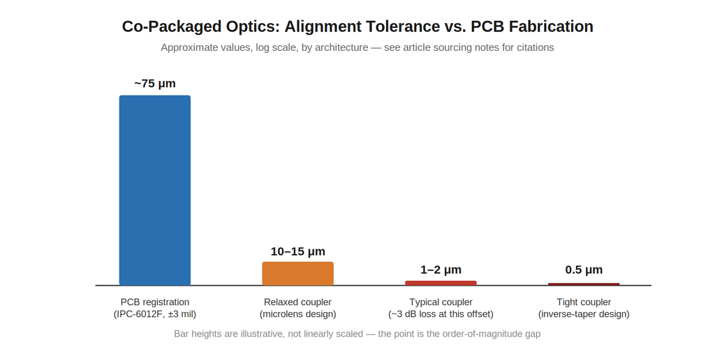
A standard single-mode fiber and a silicon-on-insulator waveguide have a mode-area mismatch exceeding 400:1, which makes fiber-to-chip coupling a dominant optical loss source in photonics packaging.¹¹ The alignment tolerance this can demand is architecture-dependent and, for the tightest designs, brutal.
For an inverse-taper spot-size converter — one common coupling architecture — a lateral offset of just 0.5 micrometers can cut coupled optical power in half.¹² Other coupling architectures relax this substantially: a microlens-based coupling design, for instance, can tolerate lateral misalignment on the order of 10–15 micrometers.¹³ A 1–2 micron translational misalignment in a more typical design costs roughly 3 dB.¹¹
This isn’t a clean apples-to-apples comparison against PCB fabrication tolerances, since the two use fundamentally different manufacturing paradigms. PCB registration is a mechanical drilling/lamination tolerance. Photonic coupling alignment is a different problem entirely, and the industry is actively engineering around its tightest version.
imec’s work on silicon nitride and polymer optical redistribution layers exists specifically to relax the sub-micron tolerance that bare edge-coupled designs demand, by expanding the effective spot size at the coupling interface.¹⁵ A separate line of packaging work — vertical couplers that expand the laser beam size — reports the same directional effect: looser coupling tolerance at the cost of some added process complexity, while also supporting wafer-scale testing.¹⁶
Separately, redistribution-layer lithography in advanced chiplet packaging has demonstrated line width and spacing down to roughly 0.5 micron, which shows that sub-micron precision tooling exists in advanced packaging generally. That’s a lithographic technique for electrical routing, though, not the same thing as active photonic alignment — it shouldn’t be read as evidence that the optical coupling problem in co-packaged optics is already solved by borrowing it directly.¹⁶
Still, for perspective: fabricator design guidance for working within IPC-6012F (the current base rigid-board specification, revised September 2023) Class 3 requirements commonly budgets around ±3 mils (roughly 75 microns) of registration allowance in practice.¹⁴ Tight-tolerance optical coupling designs, by contrast, operate in the sub-micron to low-single-digit-micron range before relaxed-tolerance coupler architectures are applied — a meaningfully different manufacturing discipline, even if a precise multiplier between the two isn’t something any single source states directly.
Engineering Breakdown
| Element | Detail |
|---|---|
| Mechanism | Optical coupling efficiency degrades sharply in tight-tolerance architectures — roughly 3 dB per 1–2 micron of misalignment in typical designs, more for bare inverse-taper couplers — because single-mode fiber and waveguide mode-field diameters mismatch by over 400:1 |
| Trade-off | Tighter alignment improves coupling efficiency and reduces packaging footprint, but drives up assembly cost and cuts yield unless relaxed-tolerance coupler designs (microlenses, SiN/polymer redistribution, vertical couplers) are used instead |
| Consequence | This is a manufacturing and assembly problem more than a device-physics problem, and it’s a significant bottleneck between demonstrated photonic links and hyperscale production — though relaxed-tolerance coupler designs are one of the industry’s active responses to it |
The Laser Reliability Problem — and How It Got Partly Solved
There’s a reliability question specific to co-packaged optics designs worth addressing directly. (This is a version of a pattern that shows up across advanced packaging generally — see our piece on the TSMC Arizona packaging bottleneck, where the same dynamic plays out one layer down: the headline constraint gets the coverage, the boring packaging and substrate layer underneath is where output actually gets capped.)
NVIDIA’s own technical materials state directly that lasers are the most failure-prone components in its silicon photonics architecture — which is exactly why the design places them on easily accessible, field-replaceable external laser source (ELS) modules on the switch front panel rather than integrating them into the sealed package.¹⁵ Trade-press reporting citing broader hyperscaler field data makes a similar general claim about laser sources being among the more common failure modes across optical systems.¹⁶
That’s part of why several major co-packaged optics vendors, including NVIDIA and Ayar Labs, have adopted External Laser Source architectures — more precisely, ELSFP, or External Laser Small Form-factor Pluggable — instead.¹⁶ ¹⁷ The laser sits in a separate, often pluggable module connected to the optical engine by fiber, preserving field servicing for the common case of laser failure. NVIDIA’s case has confirmed production evidence via both its own technical materials and the Lambda deployment discussed above; broader industry-wide adoption is real but not confirmed at the same evidentiary standard for every named vendor.
What ELSFP doesn’t solve is failure of the optical engine itself. That can still require replacing an entire line card or server board rather than swapping a single pluggable module.¹⁸ Thermal mismatch between heat-generating electronics and temperature-sensitive optical elements can also drive wavelength drift and accelerated aging — the same thermal-drift mechanism discussed in the WDM tuning-power trade-off above, now acting on device lifetime instead of link stability.¹⁹
Field data on long-term co-packaged optics reliability at hyperscale is still accumulating. It doesn’t yet match the decade-plus track record pluggable optics already carries.¹⁸
ELS architectures also shift some laser-safety analysis toward field-accessible optical interfaces and service procedures; applicable classification under IEC 60825-1 (the specific standard in that series covering laser-product classification) depends on accessible emission levels and overall system design, not simply on how many connection points exist — a topic outside the scope of this piece but one that qualification and safety engineers would reasonably expect addressed before broad deployment.
This is a pattern that repeats across advanced packaging generally: a working lab demonstration and a manufacturable process at acceptable yield can be years apart, and that gap is where the real engineering work happens.
Coexistence, Not Replacement
Copper at short reach — on-package, chip-to-chip within a module, short board traces — stays the simplest, cheapest, most mature choice for the foreseeable future. There’s no engineering reason to replace a link that isn’t failing its loss budget. (Interconnect power is only half of the facility-level power and thermal story — see our piece on why AI data center cooling is becoming the industry’s real bottleneck for the other half: what happens to all the heat once it leaves the rack.)
The more accurate way to think about the current landscape isn’t a strict distance hierarchy — it’s a spectrum of where electro-optical conversion happens and how much retiming/DSP overhead sits in the path:
- Copper — no optical conversion at all, for on-package and board-level reach where loss budgets are still comfortable
- Linear Pluggable Optics (LPO) — an intermediate technology that strips power-hungry retiming DSPs out of the optical module, extending the economic life of both copper and simpler pluggable architectures²⁰
- Co-packaged optics — electro-optical conversion moved adjacent to the switch ASIC specifically to eliminate long electrical paths inside the switch, not defined by a fixed “middle” optical distance
- Pluggable transceivers — a mature, serviceable, field-proven architecture that can serve overlapping optical reach classes with co-packaged optics; the meaningful difference is largely about integration, power, density, and serviceability rather than distance alone
Coverage that frames this as photonics eliminating copper collapses an architecture decision into a material swap. It isn’t one.
The Constraint Engineers Should Actually Watch
If there’s one number worth tracking over the next several years, it isn’t a bandwidth spec. It’s optical coupling yield at production volume — how consistently manufacturers hit their target alignment tolerance, whatever coupler architecture they’ve chosen, across thousands of units without a reliability penalty through thermal cycling, and how fast failure semantics for the optical engine itself, not just the laser, improve.
Copper didn’t get worse. The distance it can carry AI-cluster bandwidth efficiently got shorter, and the co-packaged optics industry is now solving a packaging and assembly problem to close the gap — a problem PCB and advanced packaging engineers already have relevant experience with, just at tolerances that, for the tightest coupler designs, run meaningfully past anything Class 3 board fabrication has required. Hardware teams that treat optical I/O as a first-class design constraint now — the way SerDes channel budgets became one a decade ago — will be the ones ready when their compute density finally outruns what copper can deliver.
About the Author
Imran Valiani | Sales Director, PCB Electronics Manufacturing
20+ years working with major Bay Area and global tech clients. Founder of Silicon to Software, where I write about the hardware layer — PCB fab, AI gear, autonomous systems, and cyber — the stuff most tech writers have never touched. Literally.
Follow: X @SiToSoftware | LinkedIn
For more analysis of compute, power, cooling, and infrastructure constraints, explore the AI Hardware & Data Centers Resource Hub.
This article was developed with AI assistance and edited, fact-checked, and reviewed by the author. See my full AI disclosure.
Sources
- Mike Li (Fellow, Altera/Intel; OIF Board Member), “SERDES at 224 GBps and Beyond,” OIF presentation, Oct 2024. https://146a55aca6f00848c565-a7635525d40ac1c70300198708936b4e.ssl.cf1.rackcdn.com/images/35ae8b4c1eb19b4db54821db539921539acc14ef.pdf — Additional: OIF, “448G Architectures for AI,” ECOC Market Focus 2025. https://www.oiforum.com/wp-content/uploads/OIF_448Gbps_Presentation_MarketFocus_FinalMK.pdf
- “224G PCB Design: Next Frontier for AI Data Center Interconnects,” NextPCB. https://www.nextpcb.com/blog/224g-pcb-design-ai-data-center
- “New-generation silicon photonics beyond the single-mode regime,” arXiv preprint, Apr 2021. https://arxiv.org/pdf/2104.04239
- “Towards Terabit/λ/s Multidimensional Silicon Photonic Engine,” arXiv preprint. https://arxiv.org/html/2608.11639
- “Low-latency passive thermal desensitization of a silicon micro-ring resonator with self-heating,” APL Photonics, AIP Publishing, Jul 2024. https://pubs.aip.org/aip/app/article/9/7/076117/3304765/
- “Recent Progress in Silicon-Based Slow-Light Electro-Optic Modulators,” NCBI PMC (PMC8950839). https://www.ncbi.nlm.nih.gov/pmc/articles/PMC8950839/
- “Co-Packaged Optics Reaches Power Efficiency Tipping Point,” SemiEngineering, Jul 2025. https://semiengineering.com/co-packaged-optics-reaches-power-efficiency-tipping-point/
- “Towards Terabit/λ/s Multidimensional Silicon Photonic Engine,” arXiv preprint (same as source 4). https://arxiv.org/html/2608.11639
- NVIDIA Newsroom, “NVIDIA Announces Spectrum-X Photonics, Co-Packaged Optics Networking Switches,” Mar 18, 2025. https://nvidianews.nvidia.com/news/nvidia-spectrum-x-co-packaged-optics-networking-switches-ai-factories — NVIDIA Silicon Photonics product page (accessed May 29, 2026 snapshot). https://www.nvidia.com/en-us/networking/products/silicon-photonics/ — Lambda, “Lambda at NVIDIA GTC 2026,” Mar 16, 2026. https://lambda.ai/blog/lambda-at-gtc-2026-building-the-superintelligence-cloud
- SDxCentral, “Lambda offers glimpse into Nvidia’s CPO switch,” Jun 2, 2026. https://www.sdxcentral.com/news/lambda-offers-glimpse-into-nvidias-cpo-switch-enabling-more-tokens-through-substantial-power-savings/
- “Fiber-to-chip coupling loss: 27+ patent analysis,” PatSnap. https://www.patsnap.com/resources/blog/articles/fiber-to-chip-coupling-loss-27-patent-analysis/
- US Patent 9,335,480, “Optical alignment using multimode edge couplers,” Huawei Technologies. https://patents.google.com/patent/US9335480B1
- US Patent 8,855,452, “Silicon photonic chip optical coupling structures,” IBM. https://patents.google.com/patent/US8855452B2
- Atlas PCB, “IPC Class 2 vs Class 3: Which Standard Does Your Board Need?” https://www.atlaspcb.com/blog/ipc-class-2-vs-class-3/
- IMEC, “Interfacing silicon photonics for high-density co-packaged optics.” https://www.imec-int.com/en/articles/interfacing-silicon-photonics-high-density-co-packaged-optics — NVIDIA Developer Technical Blog, “A New Era in Data Center Networking with NVIDIA Silicon Photonics-based Network Switching,” Apr 2025. https://developer.nvidia.com/blog/a-new-era-in-data-center-networking-with-nvidia-silicon-photonics-based-network-switching/
- “Why Co-Packaged Optics Uses External Lasers Instead of Integrated Sources,” industry newsletter, Nov 9, 2025. https://www.viksnewsletter.com/p/why-cpo-uses-external-lasers — ASE / SemiEngineering, “Advanced Packaging Evolution: Chiplet and Silicon Photonics-CPO.” https://ase.aseglobal.com/blog/technology/advanced-packaging-for-ai-chiplet-and-cpo/
- SemiAnalysis, “Co Packaged Optics (CPO) – Scaling with Light for the Next Wave of Interconnect,” Apr 10, 2026. https://newsletter.semianalysis.com/p/co-packaged-optics-cpo-book-scaling
- APNIC Blog, “Co-Packaged Optics — a deep dive,” May 7, 2025. https://blog.apnic.net/2025/05/07/co-packaged-optics-a-deep-dive/
- PatSnap Eureka, “How to Increase Reliability of Co-Packaged Optics Components.” https://eureka.patsnap.com/report-how-to-increase-reliability-of-co-packaged-optics-components
- OIF, “OIF Concludes Q3 2025 Member Meeting” (CEI-112G-LINEAR-PAM4 IA) and “OIF Publishes Implementation Agreement for 112 Gb/s RTLR” (EEI-112G-RTLR IA), Business Wire, 2025. https://www.businesswire.com/news/home/20250923374791/en/ and https://www.businesswire.com/news/home/20251118198285/en/
- OIF, “Implementation Agreements (IAs)” — official published IA list. https://www.oiforum.com/technical-work/implementation-agreements-ias/
- OIF, “Informative Documents.” https://www.oiforum.com/documents/informative-documents/technical-white-papers-requirements-framework-errata/





The discussion in “Co-Packaged Optics: Improving the Critical 224G Bottleneck” is clear and useful. The supporting details make the main points much easier to understand.