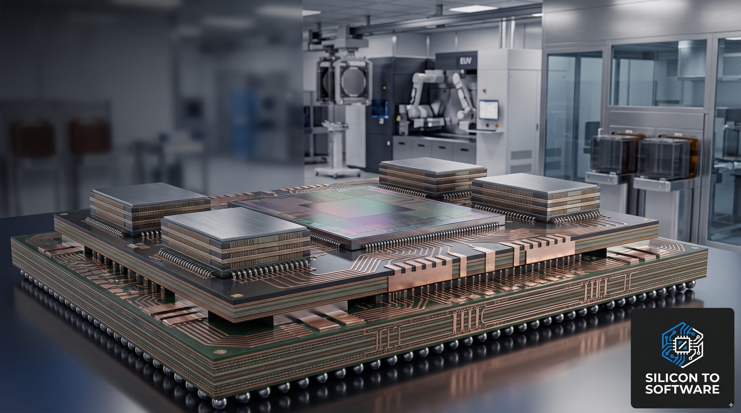
The TSMC Arizona Bottleneck Isn’t the Wafer Fab: A $265B Warning for AI Chips
For today’s leading AI accelerators, wafer fab capacity is only one constraint — CoWoS advanced packaging and IC substrate qualification cycles can set an equally binding, and at times more immediate, ceiling on output.
Table of Contents
The TSMC Arizona bottleneck isn’t where most coverage says it is. In April 2025, TSMC broke ground on its third Arizona fab, targeting the N2 and A16 process nodes — the kind of leading-edge silicon that shows up in every headline about America “onshoring” the chip supply chain. By June 2026, at TSMC’s annual shareholders meeting, CEO C.C. Wei was describing a different part of the operation entirely — not the fab, not the transistor node — as sold out through the rest of 2026: advanced packaging, specifically CoWoS.
That doesn’t make the same kind of headline. The fab groundbreaking does.
I’ve spent twenty years selling into the board and substrate side of this industry — laminates, stackups, yield curves, the parts of the business that never make the press release. (For a closer look at how laminate choice alone can make or break a design, see Choosing the Right High-Speed Laminate for AI Hardware — a different layer of the same materials-constrain-everything problem this piece is about.)
This piece focuses specifically on the leading-edge, AI-accelerator segment of the chip supply chain — CoWoS-class packaging and the substrates underneath it — not the semiconductor industry as a whole. For legacy and analog chips, wafer capacity has historically been the dominant constraint.
The U.S. Department of Commerce’s own 2021–2022 review of the global chip shortage found that wafer production capacity was “the primary bottleneck across the board,” with materials, assembly, and packaging identified as additional constraints. For today’s AI accelerators specifically, though, the balance has shifted, and the packaging and substrate layer underneath the fab deserves more scrutiny than it gets.
The TSMC Arizona Bottleneck Isn’t the Wafer Fab
When people discuss Taiwan’s chip dominance, they typically mean the wafer fab — the cleanroom with the EUV lithography systems, the facility that turns a blank silicon wafer into a die carrying billions of transistors. That’s a legitimate concentration risk. It’s just not the whole risk, at least not for the segment of the market this piece is about.
A finished, high-yield wafer is an intermediate good, not a shippable product. Before it becomes part of a GPU, an AI accelerator, or a phone SoC, it has to be diced, packaged, and mounted onto a substrate that provides both the electrical interconnect and the mechanical support for the rest of the system.
That packaging and substrate step is a distinct manufacturing discipline — different equipment, different supplier base, different yield dynamics — and its capacity does not scale on the same timeline as the fab’s. Substrate fabrication isn’t a downstream step that happens after packaging; it’s a separate input that has to arrive in parallel, made by an entirely different set of companies than the ones building the fab.
TSMC Arizona’s Buildout: What’s Actually Under Construction
The Arizona buildout is real and accelerating, and it’s worth grounding the rest of the argument in the actual numbers before complicating the picture.
Fab 21, TSMC’s first Arizona facility, entered high-volume N4 production in the fourth quarter of 2024, supplying Apple and, by multiple accounts, Nvidia and other leading customers — Apple has confirmed it as a customer directly; TSMC does not publish a complete customer roster. The second fab’s main structure was completed in 2025, with facility and equipment installation underway; TSMC has targeted high-volume N3 production for the second half of 2027. The third fab broke ground in April 2025 for N2 and A16. A fourth fab and Arizona’s first advanced-packaging facilities began initial construction in early 2026.
The CHIPS Act funding behind the original three-fab program moved from a non-binding preliminary memorandum of terms, signed in April 2024, to a finalized $6.6 billion direct-funding award in November 2024, following the Commerce Department’s due-diligence review — a binding agreement, not a pending proposal, by the time the fourth fab and packaging facilities broke ground in 2026.
The capital commitment tells its own story. TSMC’s Arizona investment started at $12 billion in 2020. By April 2024 it was $65 billion, across three fabs. By mid-2026 it was a reported $165 billion. Then, on July 16, 2026, CEO C.C. Wei announced another $100 billion, bringing the total to $265 billion across ten fabrication plants, two advanced-packaging facilities, and an R&D center.
That escalation is worth sitting with: TSMC raised its own committed number roughly four times in six years. 2026 capital expenditure guidance was raised to $60–64 billion, which, if spent as guided, would represent TSMC’s largest annual capital-spending level to date.
City and state economic development officials, and subsequent independent reporting, have put the resulting Arizona share of TSMC’s global 2-nanometer-and-beyond capacity at roughly 30 percent upon completion of all announced facilities — a figure this analysis has not been able to confirm as a direct, verbatim statement from TSMC’s own investor materials or earnings-call transcripts, though it has been repeated across multiple independent outlets.
TSMC has repeatedly increased this commitment while citing strengthening AI-driven customer demand — though geographic diversification, U.S. policy incentives, and customer localization preferences are also part of the calculus, not demand alone.
None of it is cheap. TSMC’s own CFO has stated that constructing a fab building and facilities in the U.S. runs 4 to 5 times the cost of the same construction in Taiwan. That figure describes building and facility costs specifically, not the fab’s total capital expenditure — equipment, which dominates overall capex, varies less by geography.
Leading-edge production still starts in Taiwan first. Arizona has historically trailed by roughly a node generation; the third and fourth Arizona fabs, targeting N2 and A16, suggest that gap may be narrowing, though TSMC hasn’t stated a firm timeline for reaching full node parity between the two sites.
None of this happens in a vacuum, and the specific 4-to-5x figure TSMC’s CFO has cited likely reflects more than one factor rather than a single cause. US construction labor costs are widely reported as higher than Taiwan’s for comparable large-scale industrial projects, and permitting and regulatory review timelines can differ meaningfully between the two jurisdictions — both plausible contributors to a building-and-facilities premium, though the CFO’s figure doesn’t break out how much each factor contributes individually. A newer site also starts without the dense local ecosystem of specialized subcontractors, equipment technicians, and materials suppliers that has built up around Taiwan’s fabs over decades; assembling and coordinating that support network from scratch is itself a cost and schedule factor, separate from the cost of the building itself.
The roughly one-node lag likely reflects a related but distinct set of considerations. Bringing a new process node to volume production requires more than installed equipment — it requires a workforce with hands-on experience running that specific process, together with a qualification and yield-ramp cycle that benefits from proximity to the engineering teams and suppliers most familiar with the recipe. Standing up that combination at a new site can reasonably be expected to take longer than running an already-mature process at an established one, which is one plausible reason leading-edge nodes have tended to reach Taiwan first before extending to Arizona — though TSMC has not attributed the lag to any single one of these factors in its public statements.
Why Advanced Packaging Is the Binding Constraint for AI Chips
For this segment of the market, TSMC’s advanced-packaging capacity has constrained AI accelerator output for close to two years — by several public accounts, arguably as much as or more than wafer capacity has recently.
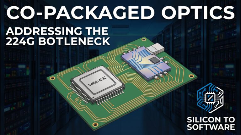
CoWoS is TSMC’s family of 2.5D packaging technologies for HPC and AI products. CoWoS-S, in production since 2012, uses a large silicon interposer and can accommodate interposer sizes up to roughly 3.3x reticle.
For larger packages — the class driving much of today’s AI accelerator demand — TSMC uses CoWoS-L, which combines a molding-based interposer with RDL routing and embedded Local Silicon Interconnect (LSI) chips for high-density die-to-die connections, alongside CoWoS-R, which uses a fully RDL-based interposer with no silicon interposer at all. Through-silicon-via formation is specific to the CoWoS-S silicon-interposer flow; it isn’t a universal step across every CoWoS variant.
All three illustrate why advanced-packaging capacity doesn’t scale automatically with wafer capacity. TSMC’s expanded July 2026 Arizona plan adds both: four more wafer fabs targeting 2-nanometer-and-below nodes, alongside dedicated advanced-packaging facilities — a tacit acknowledgment that building one doesn’t solve the other.
The CoWoS Capacity Numbers
Third-party supply-chain estimates — not figures TSMC itself discloses on a monthly basis — have put TSMC’s monthly CoWoS capacity at roughly 35,000–40,000 wafers at the end of 2024, climbing to around 75,000 by the end of 2025. TrendForce reported in June 2026 that capacity could reach a record 120,000 to 140,000 wafers by the end of 2026 — with an additional 50,000 to 60,000 wafers/month from OSAT partners potentially pushing total industry capacity toward 200,000.
At TSMC’s June 4, 2026 shareholders meeting, CEO C.C. Wei was reported as describing CoWoS capacity as “extremely tight and sold out through 2026,” a statement corroborated across multiple independent outlets citing the same event, though the exact wording hasn’t been independently verified against a webcast transcript.
That gap isn’t static. TrendForce reporting, citing Economic Daily News, has put the CoWoS supply-demand gap at roughly 20 percent as of mid-2026, narrowing toward an estimated 10 percent by year-end. TSMC has separately forecast, per remarks at its May 2026 Taiwan Technology Symposium reported by Reuters, that CoWoS capacity will grow at a compound annual growth rate of more than 80 percent from 2022 through 2027 — a multi-year growth trajectory, not an annual 2026 figure. The bottleneck is real and currently binding — but it’s on a defined trajectory, not an open-ended one.
The engineering reason matters more than the headline number: producing a CoWoS package involves interposer or interconnect-chip fabrication — much of it on front-end-adjacent wafer processing rather than in the backend packaging house itself — followed by wafer-level die and memory stacking, and redistribution-layer processing at dedicated packaging facilities. That combined process chain doesn’t scale in lockstep with wafer fab capacity. TSMC has had to build it out as its own facilities with their own multi-year ramp, regardless of how fast the fab next door is running.
The underlying reason is that wafer fabrication and advanced packaging are built around different equipment sets, different facility requirements, and different qualification cycles, even when they sit on the same campus. A wafer fab’s cleanroom and lithography tools have no direct application to interposer processing, die-stacking, or the inspection and test equipment a CoWoS line depends on; expanding one doesn’t create spare capacity in the other. Packaging capacity also carries its own yield-learning curve, distinct from the wafer-level yield discussed elsewhere in this piece, since bonding and stacking introduce failure modes that don’t exist during wafer processing. That’s part of why TSMC can add wafer capacity at one pace while advanced-packaging capacity lags behind on a slower, separately-financed schedule of its own.
The IC Substrate Bottleneck: ABF Film and a Concentrated Supplier Base
Go one layer further down, and this is the part of the chain almost no general-audience coverage names. It’s worth being precise about what “my industry” means here: the vocabulary overlaps with traditional PCB manufacturing — laminate selection, stackup design, CTE matching — but IC substrate fabrication, with ABF build-up film, laser-drilled microvias, and semi-additive metallization, is a distinct and more demanding discipline than standard PCB production. The overlap is real; it isn’t identical.
Many high-performance packages, including current CoWoS implementations, sit on an organic substrate built from ABF (Ajinomoto Build-up Film), an insulating dielectric layer. High-end FC-BGA (flip-chip ball grid array) substrate fabrication is concentrated among a small group of manufacturers that includes Ibiden, Shinko Electric, Unimicron, AT&S, and Nan Ya PCB, alongside other suppliers such as Samsung Electro-Mechanics and Kinsus in specific segments. For TSMC’s own CoWoS flow, silicon interposer processing is integrated into TSMC’s advanced-packaging manufacturing network.
Beneath the substrate-fabrication tier sits a further chokepoint: the ABF film itself comes almost entirely from a single Japanese producer. That producer’s manufacturing footprint is currently limited to two plants, both in Japan — though the company announced in May 2026 that it had acquired land in Gifu Prefecture for a third production site, with construction slated to begin in 2028 and operations targeted for 2032.
Ajinomoto’s own materials describe the company’s position in the relevant interlayer-insulation market as roughly 95 percent to near 100 percent, depending on how the market is defined. That’s a company-stated figure, not an independently audited one — worth remembering given how much of the concentration argument in this piece rests on it.
What the 2021–2022 ABF Shortage Taught the Industry
This isn’t a hypothetical risk. It already happened once. Through 2021 and into 2022, industry reporting put ABF substrate supply roughly 20 percent short of demand, with the shortage expected to ease as new capacity came online through 2023, according to the chairman of one of Taiwan’s leading IC substrate manufacturers.
Multiple suppliers — Unimicron, Nan Ya PCB, Kinsus, Ibiden, Shinko, and AT&S — brought new ABF capacity online simultaneously, and reporting at the time noted that higher layer counts on newer processors meant longer stacking process times and tighter yield margins, both of which capped real output growth even as nominal capacity expanded.
Whether that 2021 easing timeline actually held is worth flagging honestly: later reporting suggests the highest-end AI/HPC segment of the substrate market still hadn’t reached full equilibrium by early 2025, even as broader consumer and PC substrate segments eased — meaning the original 2021 guidance may have been optimistic specifically for the AI-relevant end of the market.
That concentration isn’t going unaddressed, either. Ibiden’s board approved a capital investment plan of approximately ¥500 billion for its electronics business across fiscal years 2026–2028, with the first phase — roughly ¥220 billion — targeted specifically at expanding production capacity for high-performance IC package substrates used in AI and high-performance servers. Ajinomoto has its own capacity expansion underway, including the new Gifu site. Neither company has disclosed a specific resulting output multiplier in its own materials; whether the combined expansion outpaces AI-driven demand growth is the open question worth tracking, not whether anyone is trying to close the gap.
The practical lesson for anyone sourcing components: qualifying a new substrate supplier is not simply a capital problem solved by writing a check and setting a deadline. It’s fine-line/space capability, CTE-matched laminate stacks, warpage control at panel level, and a yield-learning curve — qualification and yield ramp can run from many months to, for demanding new process/product combinations, multiple years, varying by package architecture, layer count, and customer reliability requirements.
CTE mismatch between die and substrate drives interfacial stress that can lead to delamination or solder-joint fatigue over thermal cycling; warpage beyond spec causes coplanarity failures during reflow and yield loss at assembly. That’s the failure mode underneath the abstraction “qualification takes time” — and it’s a clock that doesn’t compress the way a construction timeline does.
It’s the same tolerance-stack discipline that governs common PCB DFM mistakes at the board level — annular ring, registration, trace geometry — just applied at a finer pitch and a higher stakes level.
Has TSMC Actually Closed the Gap? Stress-Testing the Diversification Story
The skeptics who argued in 2020 that none of this could be replicated outside Taiwan on any reasonable timeline have been proven partly wrong, and any honest analysis has to account for that. Reported build timelines for TSMC’s overseas fabs have compressed from roughly three years for the first Arizona phase to an estimated 1.5 to 2 years for later phases — though the exact construction milestones being compared (groundbreaking to shell completion, versus groundbreaking to volume production) aren’t always specified in the underlying reporting, so this comparison should be read as directional rather than precise.
Major U.S. customers including Apple, Nvidia, AMD, and Qualcomm have reportedly factored geopolitical considerations into their sourcing decisions as TSMC’s overseas footprint expands.
One data point is worth naming directly. On May 18, 2026, an industry publication (SoftwareSeni) reported that Arizona packaging capacity “is not on the cards until 2029.” On July 16, 2026, TSMC announced two advanced-packaging facilities as part of its $265 billion Arizona commitment, with construction on the first having already begun months earlier, in early 2026, according to TSMC’s own materials. That May prediction wasn’t a fringe rumor, but it also wasn’t right — and it was overtaken by events within ten weeks of publication.
What hasn’t moved is the construction-cost premium and the substrate qualification cycle. Diversification is real and accelerating. Full parity — in leading-edge capacity, packaging depth, and the surrounding supplier ecosystem — is not close, and the two claims are not interchangeable.
Silicon Shield: Separating Economic Fact From Strategic Speculation
The economic concentration is documented fact: Taiwan’s fabrication and substrate ecosystem sits at the center of a supply chain the rest of the world depends on. Whether that concentration functions as a deterrent against military conflict is a different question, one outside the scope of hardware-industry expertise, and this piece deliberately stays on the supply chain side of that line. Readers looking for the geopolitical/military analysis should look to sources with that specific domain background — the engineering and manufacturing claims here stand independently of it.
The Practical Takeaway for Hardware Engineers
If you build hardware for a living, the real TSMC Arizona bottleneck isn’t Taiwan geopolitics — it’s your own bill of materials. Every team stress-tests the exotic part — the FPGA, the RF front end, the custom ASIC. Fewer teams map how many of the “boring” line items — substrates, laminates, dielectric films — trace back through a genuinely small number of qualified suppliers, in some cases concentrated in the same country or region.
The U.S. Department of Commerce’s own 2021–2022 review of the global chip shortage found that wafer production capacity was the primary bottleneck overall, with materials, assembly, and packaging identified as additional constraints. ABF substrate supply was one of those additional constraints — real, underappreciated, and capable of capping output for CPUs, GPUs, and networking silicon even when die capacity was available, but not the primary driver of the broader shortage.
That distinction is the more useful lesson, not a less interesting one: even a genuinely secondary constraint, in an obscure material almost no engineer had heard of, was enough to cap output for entire product categories. The layer that gets ignored in a supply chain review doesn’t have to be the biggest one to be the one that breaks first.
About the Author
Imran Valiani | Sales Director, PCB Electronics Manufacturing
20+ years working with major Bay Area and global tech clients. Founder of Silicon to Software, where I write about the hardware layer — PCB fab, AI gear, autonomous systems, and cyber — the stuff most tech writers have never touched. Literally.
Follow: X @SiToSoftware | LinkedIn
For more analysis of chip scaling, advanced packaging, memory, and semiconductor engineering constraints, explore the Semiconductor Engineering & Advanced Packaging Resource Hub.
This article was developed with AI assistance and edited, fact-checked, and reviewed by the author. See my full AI disclosure.
Sources
Primary company and technical documentation:
- TSMC, official Arizona project page — tsmc.com/static/abouttsmcaz
- TSMC, CoWoS technical documentation — 3dfabric.tsmc.com
- TSMC, press release on preliminary CHIPS Act funding terms, April 8, 2024 — pr.tsmc.com
- Ajinomoto / Ajinomoto Fine-Techno, press release on new Gifu production site, May 7, 2026 — news.ajinomoto.co.jp
- Ibiden Co., Ltd., notice regarding capital investment plan for high-performance IC package substrates, February 3, 2026 — ibiden.com
Government and regulatory sources:
- U.S. Department of Commerce, “Results from Semiconductor Supply Chain Request for Information,” January 25, 2022 — commerce.gov
- U.S. Department of Commerce, “Biden-Harris Administration Announces CHIPS Incentives Award with TSMC Arizona,” November 15, 2024 — commerce.gov
Industry research and reporting:
- TrendForce, “TSMC CoWoS Supply-Demand Gap Reportedly Seen Narrowing from 20% to 10% by End-2026 as Capacity Expands,” June 15, 2026 — trendforce.com
- TrendForce, reporting on TSMC Arizona build-timeline compression and customer sourcing considerations, March 2026
- SoftwareSeni, “TSMC CoWoS Packaging the Silent Bottleneck in the AI Chip Supply Chain,” May 18, 2026
- DigiTimes and Tom’s Hardware, contemporaneous reporting on the 2021–2022 ABF substrate shortage
- NVIDIA Corp. (NVDA) Q4 FY2026 Earnings Call transcript, February 25, 2026 (FactSet CallStreet) — reviewed directly to verify sourcing of packaging-related claims attributed to Nvidia management
Company-stated figures (TSMC’s construction-cost comparisons, Ajinomoto’s market-share claims, the ~30% Arizona capacity projection) are identified as such throughout and should be read as claims made by the companies or reported by secondary sources, not independently audited figures, except where a primary filing is cited directly.