
5 Common PCB DFM Mistakes That Can Reduce Fabrication and Assembly Yield
Five common PCB Design for Manufacturability (DFM) mistakes that can increase fabrication costs, reduce yield, delay production, and create assembly problems — and how experienced PCB engineers catch them before a design is released.
Table of Contents
These five PCB DFM mistakes show up on design after design, in two decades of working with engineering teams at a Silicon Valley PCB manufacturer. Funded startups. Established OEMs. Doesn’t matter.
They’re not exotic failures. They’re common ones, and common is exactly what makes them expensive — because everyone assumes someone else already checked for them.
Here’s the thing — most yield problems get blamed on the fab house. But by the time a board hits the panel, the die is usually already cast. DFM is where the real battle happens. Let’s walk through the five mistakes I see most and how to catch them before the manufacturing data package goes out the door.
1. Ignoring Copper-to-Edge Clearance
This one bites beginners the hardest because it’s invisible until it isn’t.
When copper features — traces, pads, pours — sit too close to the board’s physical edge, routing or scoring during panel separation can expose, damage, or deform that copper. Sometimes it shorts against a mounting bracket. Sometimes it just tears away entirely.
This kind of problem is usually caught by mechanical DRC or the fabricator’s CAM review — not by electrical or signal-integrity simulation, which isn’t built to look for it in the first place.
What actually happens during separation
- Routing bits generate mechanical stress along the board perimeter
- V-scoring removes material from both surfaces and leaves a residual web; anything the score line intersects is at risk
- Unintended copper inside the minimum clearance zone can be exposed, cracked, or deformed when the board comes off the panel
One caveat worth flagging: not all edge copper is a mistake. Edge plating, castellations, and card-edge contacts intentionally put copper at or near the edge — but they require separate, controlled design rules and explicit fabrication notes, not a default clearance.
IPC-2221C (the current generic printed-board design standard) provides generic conductor-to-edge design requirements, but the fabricator’s published copper-to-edge rules should control the actual release limits for your selected routing or scoring process. Follow the fabricator’s specified clearance, since it reflects that supplier’s routing, scoring, registration, and layer tolerances — it may be more restrictive than the generic design baseline.
2. Insufficient Annular Ring on Plated Through-Holes
How much copper actually needs to survive around a drilled hole for that via to stay reliable?
Not as much as people assume — but not zero, either. The land diameter has to accommodate the full manufacturing tolerance stack, not just the nominal drill size. That stack includes drill positional accuracy, artwork and layer registration, lamination movement, and plating allowance, among other factors.
If the annular ring breaks out, that’s a registration and land-condition problem. Whether it’s a defect at all — and how severe — depends on:
- Product class (Class 2 vs. Class 3 tolerances differ)
- Whether the breakout is on an external or internal land
- Whether it affects the conductor junction
- The applicable IPC-A-600 acceptance criteria and IPC-6012 performance requirements for that board
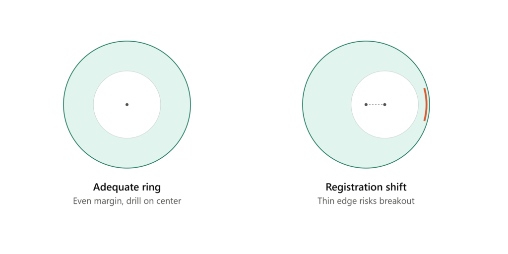
There’s no single universal rule where any breakout equals automatic rejection — it’s conditional on the board’s product class and procurement documentation. That distinction matters more in some applications than others: a Class 3 board destined for a satellite, where there’s no pulling the unit for rework once it’s in orbit, tolerates far less ambiguity than a consumer Class 2 design. What breakout can indicate is a broader registration problem worth investigating. And if it shows up alongside poor barrel plating or inner-layer connection loss, it can contribute to longer-term reliability risk, particularly under thermal cycling — the same CTE-mismatch mechanism I cover in depth in Industrial IoT Hardware Reliability. On its own, though, external breakout isn’t proof a via will fail in the field.
External and internal breakout also differ in how — and when — anyone actually catches them. External breakout sits on an outer layer, so it’s at least potentially visible to inspection depending on the board’s construction and what inspection method is applied; whether it’s acceptable still comes down to remaining copper connection and the applicable product-class criteria. Internal breakout is buried inside the stack-up. It isn’t observable from the finished surface, so confirming its condition typically depends on cross-section analysis, electrical test, or other inspection methods capable of reaching a buried layer — not a visual check of the finished board. That doesn’t make internal breakout automatically worse or external breakout automatically safe; it just means the two failure modes get caught differently, and a board can pass what visual inspection catches while an internal condition goes unconfirmed without the right test method applied.
The fix isn’t glamorous
Size your pads with the full tolerance stack in mind, not just the drill diameter. Boring advice. Saves boards.
3. Solder Mask Slivers and Pad-Definition Confusion
This mistake is sneaky because it looks cosmetic. It isn’t — but the failure chain is more mundane than it sounds.
When solder mask clearance around adjacent pads is too tight, you get a thin mask web between them — especially on fine-pitch parts. If that web falls below the fabricator’s process capability, it may not image consistently, or the fabricator may simply remove it during CAM and combine the openings into one gang aperture. That’s the more common outcome, not a dramatic sliver breaking loose during reflow. The practical risk is increased solder-bridging exposure between the now-connected pads, not debris traveling to a random spot on the board.
The tighter your pitch, the less margin you have for error. Simple as that.
Two more things worth separating clearly, because they get conflated constantly:
- Via tenting covers a via opening with solder mask. It reduces exposed copper and can help limit solder wicking and contamination — but for larger apertures it doesn’t guarantee a fully sealed barrel. If via-in-pad reliability matters, specify the actual plugging, filling, or capping process instead of assuming generic tenting covers it.
- Pad definition — solder-mask-defined (SMD land) vs. non-solder-mask-defined (NSMD) — is a separate decision about BGA land geometry. NSMD is commonly preferred at the board level because solder can wet the pad’s sidewalls, but the component manufacturer’s land-pattern recommendation and the assembly process are what actually control the choice, not a universal default.
IPC-SM-840 is worth knowing about here, but it governs solder mask material qualification and performance — not which land style is safer for a given BGA. That decision comes from the component supplier’s guidance, reviewed against your fabricator’s and assembler’s capability.
4. Assembly-Panel Design Gets Bolted On Too Late
Design-for-assembly considerations — not pure bare-board fabrication — are where this next mistake lives, and it’s worth naming that distinction up front.
Panel and array decisions affect:
- Tab and mouse-bite spacing — too tight, and depaneling stresses fragile components near the break line
- Fiducial placement — missing or poorly designed fiducials can reduce registration accuracy for stencil printers, placement machines, and inspection systems, not just pick-and-place
- Assembly rail design — inadequate or inconsistent rails can interfere with conveyor support, clamping, and handling equipment
Why does this matter? Because assembly houses run boards through automated equipment at speed, and equipment compatibility depends on more than one dimension — panel flatness, edge clearance, tooling holes, and clamping geometry all factor in too.
One nuance: in a lot of supply chains, the fabricator or assembler owns and finalizes the actual production panel using their own equipment constraints. The design team’s job is to account for panel-level constraints early — keep-out zones near edges, component placement relative to likely break lines — not to hand over a finished panel drawing. Treat it as an early conversation with your assembler, not a solo design task.
5. Trace Geometry — One of the Most Common PCB DFM Mistakes
This is the classic one. The mistake that looks like a rookie error but somehow still shows up on senior engineers’ boards too.
Designers often route traces based on what CAD software allows rather than what the fabrication process can reliably produce. A few things that go wrong as a result:
- Acute trace junctions and copper neck-downs — sharp re-entrant geometry, isolated slivers of copper, or local neck widths that approach the fabricator’s imaging and compensated-etch limits. The old “acid trap” warning about every 90-degree corner is largely outdated for modern commercial etching processes; the real risk today is acute, re-entrant geometry and features that challenge the fab’s compensated etch capability, not routine right-angle bends. There’s no universal angle where a feature suddenly becomes unmanufacturable — it depends on neck width, copper thickness, layer, and the specific fab’s process capability.
- Spacing violations — minimum trace and space depend on layer type, starting and finished copper weight, imaging technology, and etch process margin, not copper weight alone
- Impedance mismatches — controlled impedance has to be derived from the fabricator-approved stack-up and modeled with the actual dielectric constant, copper thickness, and geometry, not copied from a generic CAD default. This is where laminate selection stops being a background material choice and starts driving manufacturability — dielectric loss, resin content, and glass weave all factor into both signal integrity and fab yield.
For current-carrying capacity specifically, IPC-2152 remains the dedicated IPC reference — it models conductor sizing against required current and acceptable temperature rise more directly than IPC-2221C’s generic spacing guidance. That distinction isn’t academic in high-current applications like automotive power delivery networks, where undersized conductors mean real thermal margin lost. That current-carrying math gets even more consequential once you move off copper entirely — printed conductive ink can run several times copper’s resistivity depending on the sintering method, which is exactly the kind of conductor-sizing problem IPC-2152 is built to catch. I go through the actual resistivity numbers in Printed Electronics vs. Flexible PCB: What Conductive Ink Can and Can’t Replace. IPC-2152 is currently classified by IPC as “No Longer Maintained” in its standards revision table (its original 2009 edition is still the version sold and referenced, but it isn’t under active revision). IPC-2221C still governs the broader electrical-spacing rules; neither one replaces your fabricator’s minimum producible trace-and-space limits.
A short checklist before you release the manufacturing data package
- Confirm minimum trace/space against your fab’s actual capability, not the design-rule default
- Check acute trace junctions and copper neck-downs, not every 90-degree bend
- Verify conductor sizing for current against IPC-2152, not IPC-2221 alone
Why These Mistakes Keep Happening
None of these five mistakes require exotic knowledge. That’s what makes them so persistent.
Design tools can catch a lot of this — but only when supplier-specific rules are actually configured, and DRC violations are treated as release blockers rather than warnings to wave through under deadline pressure.
The biggest shift I’ve seen in engineering teams that improve their yield: they stop treating DFM as a final gate before manufacturing and start treating it as an ongoing conversation with their fab and assembly partners, from the first layout pass onward.
Is that more work upfront? Sure. But which costs more — an extra design review cycle, or a failed panel run three weeks before a product launch?
Final Thought
Yield problems rarely come from one dramatic failure. They come from small, repeatable oversights that compound across a panel of boards. Size the annular ring for the full tolerance stack. Respect edge clearance — intentional or not. Loop in your assembler on panel constraints early. Match your trace geometry, and your current-carrying conductors, to what the fabricator can actually build and what the applicable standard actually covers.
None of it is complicated. It just requires discipline; most teams skip under deadline pressure.
About the Author
Imran Valiani | Sales Director, PCB Electronics Manufacturing
20+ years working with major Bay Area and global tech clients. Founder of Silicon to Software, where I write about the hardware layer — PCB fab, AI gear, autonomous systems, and cyber — the stuff most tech writers have never touched. Literally.
Follow: X @SiToSoftware | LinkedIn
This article was developed with AI assistance and edited, fact-checked, and reviewed by the author. See my full AI disclosure.
Standards and Further Reading
For the full current-revision list, see IPC’s official standards store.
- IPC-2221C — Generic Standard on Printed Board Design (foundation design standard for the IPC-2220 series; current revision, released December 2023, supersedes IPC-2221B). IPC’s own product listing confirms Revision C’s scope directly covers edge-board plating and minimum electrical clearance — the basis for this article’s copper-to-edge discussion.
- IPC-2152 — Standard for Determining Current Carrying Capacity in Printed Board Design (dedicated conductor-sizing reference; the original 2009 edition remains the version sold and referenced by IPC, though IPC’s own standards revision table currently classifies it as “No Longer Maintained”)
- IPC-A-600M — Acceptability of Printed Boards (current revision, released May 2025, supersedes IPC-A-600K; visual acceptance criteria — check the applicable product class before treating any condition as an automatic rejection)
- IPC-6012F — Qualification and Performance Specification for Rigid Printed Boards (current base revision, September 2023; governs performance requirements alongside IPC-A-600’s visual criteria)
- IPC-SM-840E — Qualification and Performance of Permanent Solder Mask (current revision, December 2010; material qualification, not pad-definition design guidance)
- Eurocircuits’ published copper-to-edge tolerances — a real-world example of a fabricator-specific edge-clearance rule tighter and more detailed than the generic IPC baseline: 0.25 mm on outer layers with break-routing, 0.40 mm on inner layers, and 0.45 mm where V-cut scoring is used — directly illustrating this article’s point that fabricator-published limits, not the generic standard, control actual release clearances.
Note: specific numeric tolerances (exact clearance values, drill registration figures, minimum mask-web dimensions) vary by fabricator and were intentionally left general rather than estimated. Confirm exact specs and current standard revisions with your PCB fabrication and assembly partners before finalizing a design.