Smartphone Camera Hardware Explained: Why Megapixel Count Isn’t the Full Story
Sensor size, pixel binning, stacked CMOS architecture, and computational imaging determine image quality more than the resolution number on the spec sheet.
Table of Contents
Smartphone camera hardware doesn’t work the way the spec sheet implies. You upgrade from a 12MP phone to one with a 200MP sensor, and you expect the jump to feel obvious. It doesn’t. In daylight, the photos look about the same. Indoors, at night, the new phone sometimes loses.
That gap isn’t a marketing lie. It’s a marketing incompleteness. The number on the box was never the number that determines image quality by itself.
On Samsung’s ISOCELL HP2 — the 200-megapixel sensor that has run the main camera on every Galaxy Ultra since 2023, including the current Galaxy S26 Ultra — the default output is roughly 12MP, not 200MP; full resolution exists as a selectable, non-default mode, not the default. Full-resolution mode can hold onto more spatial detail in bright, static scenes; binned output tends to win on noise and dynamic range as light drops. Those are different optimization targets, not one mode being flatly “worse” than the other.
This article breaks down why: the sensor architecture that quietly shrinks that 200MP number down to something usable, the physical limits on photosite size that no sensor generation has engineered around, the mechanical constraint inside the phone that caps how large a sensor can get, and the computational imaging pipeline that now does as much work as the optics themselves. The key technical claims below are tied to manufacturer documentation, peer-reviewed research, or independent testing, with engineering inferences identified as such.
How Pixel Binning Turns 200 Million Photosites Into a 12-Megapixel Photo
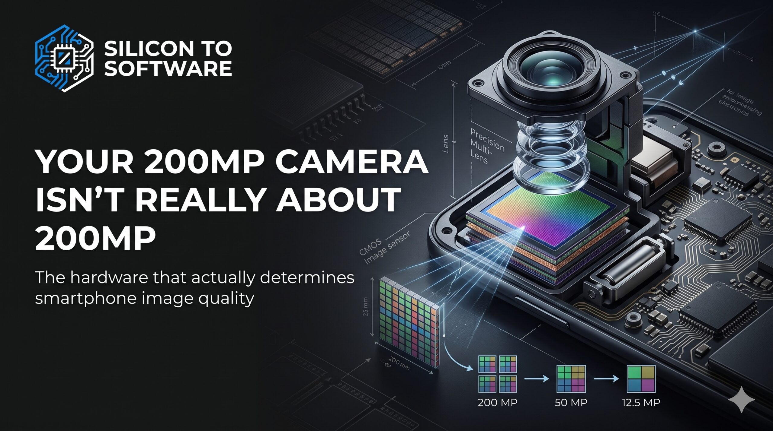
Samsung shipped the first mainstream mobile version of this technique, Tetracell, in 2017 — a 2×2 array that merges four neighboring photosites into one effective pixel. Pixel binning itself is an older, more general sensor technique; Samsung’s contribution was bringing it to mobile at scale. By 2020, the 108-megapixel ISOCELL Bright HM1 introduced Nonacell, a 3×3 scheme that merges nine 0.8-micron photosites to mimic a single 2.4-micron pixel; that nine-pixel bin reduced the 108-megapixel native sensor to a 12-megapixel output. Samsung’s own engineering disclosure for the HM1 is direct about the cost of this: as the number of merged photosites grows, so does color crosstalk between them.
Samsung didn’t invent a new fix for that problem specifically — it used ISOCELL Plus, a pixel-isolation technology the company had already introduced in 2018, to keep the higher-ratio binning practical. Binning at higher ratios still isn’t a free lunch — it’s a harder manufacturing and signal-processing problem the sensor has to actively correct for, even with that isolation technology in place.
Samsung’s first 200-megapixel sensor, the ISOCELL HP1, was introduced in 2021 with Tetra²pixel, capable of 2×2, 4×4, or full-pixel readout depending on shooting mode and available light. The sensor that actually matters here is the related ISOCELL HP2, introduced with the Galaxy S23 Ultra in 2023.
According to Samsung’s own product documentation, the HP2 defaults to 16-to-1 binning for a roughly 12.5-megapixel output, can shift to 4-to-1 binning for a 50-megapixel image in better light, and offers full 200-megapixel capture as a selectable, non-default resolution mode. That’s not a dated example: independent review confirms the HP2 sensor remains in the Galaxy S26 Ultra, Samsung’s current flagship as of this writing, with the main-camera aperture widened from f/1.7 on the previous generation to f/1.4 on the S26 Ultra. Three years of flagship phones running on one sensor design is its own data point about how incremental sensor-hardware progress actually is, compared to how often the marketing language around it changes.
Binning doesn’t make any individual photosite physically bigger — each one still only collects the photons that land on its own small area during the exposure, and the sensor die itself doesn’t change. What binning does is combine the electrical signal from several of those small photosites after the fact, so the resulting output pixel behaves, in terms of sensitivity and noise, like a single larger pixel would have — without physically enlarging anything. You trade native resolution for that gain. The full-resolution mode is built for scenes where cropping headroom matters more than light-gathering — a landscape in daylight, a product shot under studio lighting — not for what fires when you tap the shutter under ordinary conditions.
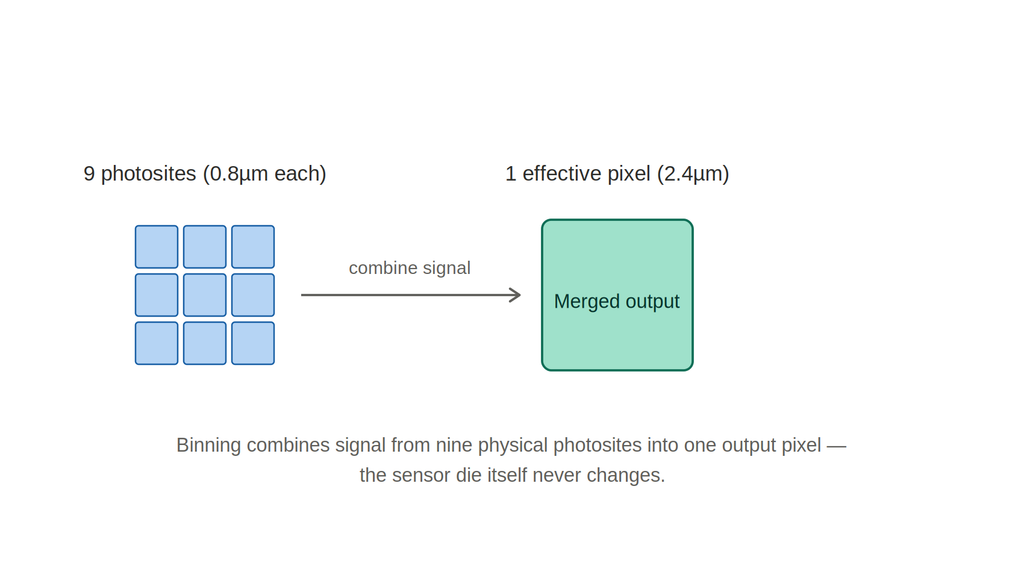
Which means the megapixel number on the spec sheet describes the sensor’s manufactured resolution, not the resolution of the photo you’ll actually get. Comparing two phones by megapixel count alone tells you nothing about how they’ll behave in the lighting conditions where most photos are actually taken.
Why Smaller Photosites Struggle Where It Counts
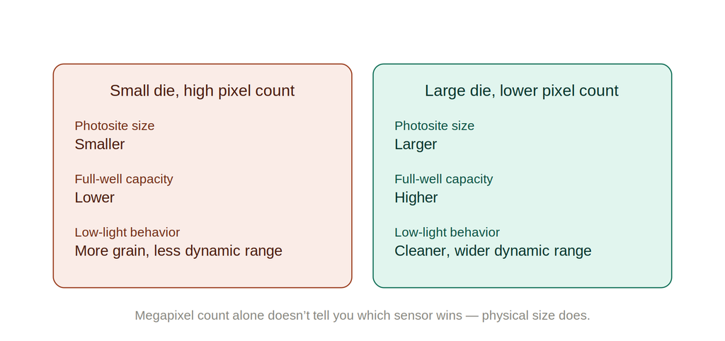
Binning exists because of a constraint no sensor generation has designed around: on a die of fixed physical size, adding more photosites means each one gets smaller.
A photosite is a light bucket, though the size of the bucket isn’t the whole story — the plumbing matters too. All else equal, larger photosite area generally provides greater full-well capacity — the maximum number of photoelectrons it can store before saturating, which caps achievable dynamic range at the bright end. Full-well capacity isn’t the only variable behind signal-to-noise ratio at a given exposure — quantum efficiency, dark current, and photon shot noise all factor in too — but it’s a major one.
“All else equal” is doing real work in that sentence, though: Sony’s own documentation for its 2-Layer Transistor Pixel architecture, presented at the IEEE International Electron Devices Meeting (IEDM) in December 2021, reports that separating the photodiode and the pixel transistor onto different substrate layers roughly doubles saturation signal level on a 1-micrometer-squared equivalent basis, compared with Sony’s own prior back-illuminated sensor design — meaning architecture, not just raw photosite area, can materially change how much signal a pixel is able to hold. A smaller photosite still collects fewer photons per unit time than a larger one built the same way, and at low light levels, where photon count is already scarce, its signal sits closer to the sensor’s read noise floor. That shows up in the image as visible grain and compressed dynamic range.
For a fixed die size, you get more photosites, or you get bigger photosites. Not both. A 200-megapixel sensor on a small die and a 12-megapixel sensor on a much larger die can produce meaningfully different low-light results, and the megapixel comparison tells you almost nothing about which one wins — the sensor’s physical size and the resulting photosite dimensions tell you far more. It’s the same shape of physical ceiling the rest of the semiconductor industry hit first at the transistor level — Moore’s Law didn’t stop; it moved from the transistor to the package once lithography ran into atomic-scale limits, and image sensors are running into a smaller-scale version of the same wall: past a certain point, the die’s physical footprint is the ceiling, not the fabrication process.
That physical format — quoted as, for instance, 1/1.3-inch (a legacy designation inherited from old video-camera tube sizing, not a literal sensor diagonal measurement) — is one of the more useful hardware clues to low-light potential, especially when comparing otherwise similar camera systems. DXOMark’s own sensor-size analysis, published in 2023, makes the case concretely: Apple roughly doubled the light-sensitive sensor area between the iPhone 12 Pro Max and the iPhone 15 Pro Max across three generations, a gain equivalent to one stop of light.
In that same 2023 comparison, the Oppo Find X6 Pro’s sensor area came in roughly double that of the iPhone 15 Pro Max — a cross-brand gap in the same year, not a generational improvement Oppo made on its own prior model, but the same underlying point: the meaningful variable was physical sensor area, not pixel count, since a larger sensor doesn’t necessarily carry more pixels. Sensor format doesn’t headline marketing copy as often as megapixel count does, and it isn’t the only variable that matters — DXOMark’s own analysis is explicit that a larger sensor alone doesn’t guarantee a better camera — but among hardware specs taken in isolation, it’s one of the more predictive ones.
The honest counterpoint: when resolution increases without shrinking the sensor — when a manufacturer pairs a higher pixel count with a proportionally larger die — you don’t sacrifice photosite size to get the extra detail. Some current high-resolution sensors are built exactly this way, and in that case, MP count and per-pixel performance improve together. Dismissing resolution as irrelevant would be its own oversimplification. The argument here isn’t against resolution as an engineering variable. It’s against resolution reported with no sensor-size context attached.
The Mechanical Constraint Marketing Copy Never Mentions
If bigger sensors with bigger photosites are generally better, the reason manufacturers don’t just build them bigger across the board is mechanical, not optical — and it’s a constraint I deal with constantly in PCB and enclosure design: available volume.
A camera module isn’t just the sensor. It’s the sensor, the lens stack above it, the OIS actuator that physically moves the lens assembly, and the housing that holds all of it in tolerance. Every one of those has a minimum z-height, and for a comparable field of view, a larger sensor generally pushes the optical design toward a longer focal length and a larger lens system — which grows the module’s total height.
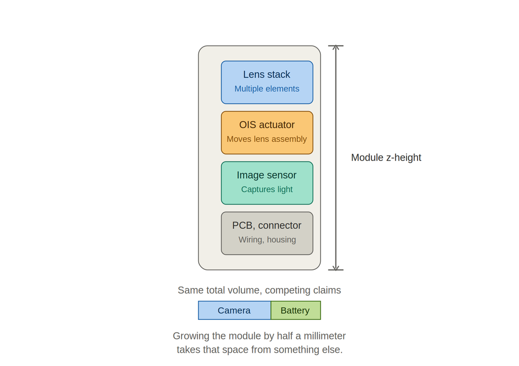
That height competes directly with two things industrial design is also fighting for: device thickness and battery volume. A module that grows by half a millimeter takes that space from somewhere — a thinner battery, a thicker phone with a more prominent camera bump, or a cut to OIS travel range that limits stabilization. It’s the same fight in a much smaller arena on smart glasses, where the camera, battery, antenna, and processor are all competing for space inside a temple arm a fraction the size of a phone chassis — the phone version of this constraint is comparatively spacious by comparison.
In my experience, sensor-size decisions on a flagship phone are effectively a negotiated outcome between the camera team wanting more light-gathering area and the industrial design and battery teams holding the line on thickness and capacity — no manufacturer publishes this process in those terms, so treat it as informed inference rather than a disclosed fact.
What’s independently observable is the pattern it would predict: sensor size grows in small, hard-won increments generation over generation — three years on the same HP2 sensor design, as noted above, is a good example — while pixel count can be increased without proportionally growing the sensor’s physical footprint, making it an easier spec to scale on paper. That doesn’t make it free, though: more pixels raise the demands on lens resolving power, sensor readout bandwidth, ISP throughput, and noise management, which is part of why the binning and on-chip processing described earlier had to get more sophisticated as resolution climbed.
Where the Real Competition Moved: Computational Imaging
None of that explains why some phones with modest sensor specs still take good photos. That part of the story is computational.
Stacked CMOS architecture — sensor logic bonded beneath the pixel array rather than sitting beside it — is common across modern flagship sensors generally. A further, less universal refinement of that same category adds a dedicated DRAM layer for frame buffering, which is the specific version relevant here. Sony’s engineers first presented this DRAM-augmented design at the IEEE International Solid-State Circuits Conference (ISSCC) in February 2017 — a 1/2.3-inch, 20-megapixel, three-layer stacked back-illuminated sensor with an integrated DRAM layer acting as frame memory — then followed with a more detailed pixel/DRAM/logic architecture at IEDM that December. Per the IEDM paper’s abstract, three silicon substrates are bonded together and connected by through-silicon vias, with the DRAM layer thinned to roughly 3 microns while retaining sufficient memory retention and operating characteristics. The stated purpose was decoupling the sensor’s internal pixel readout speed from its output interface speed, which reduces rolling-shutter distortion and enables high-frame-rate capture.
It’s the same 3D-integration category — dice stacked vertically and connected through TSVs rather than routed laterally on a shared interposer — that’s reshaping AI accelerator packaging for entirely different reasons; a camera sensor turns out to be one of the more overlooked places that same packaging approach already shipped at consumer volume.
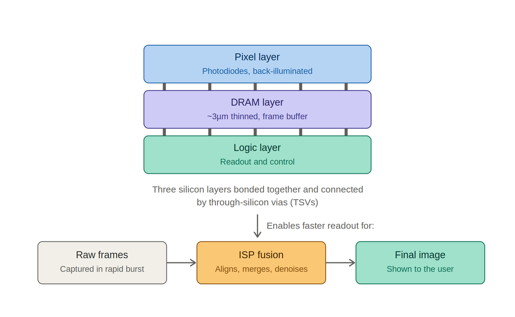
That’s not, however, what made computational photography possible in the first place. Google’s HDR+ — the multi-frame burst technique behind Night Sight and most of what Pixel phones became known for — shipped on the Nexus 5 and 6 back in 2014, and Google’s published research describes aligning and merging multiple Bayer raw frames on ordinary phone hardware, years before Sony’s DRAM-stacked sensor existed.
Multi-frame computational fusion doesn’t require a DRAM-stacked sensor. What a faster-reading stacked sensor does provide is better raw material for that computational pipeline — tighter alignment between frames, less rolling-shutter smear on anything that moved during the burst, and headroom for higher frame rates — a real, valuable contribution, just not a gatekeeping one. The same shift shows up beyond photography: Google says Pixel 8’s face unlock reached Android’s strongest biometric class using the regular front camera and machine learning rather than dedicated infrared hardware — a trade-off that changes how it behaves in the dark.
Computational imaging trades processing time and power draw for quality gains pure optics can’t deliver alone. It also means the photo you see was algorithmically reconstructed from multiple raw captures, not a single direct exposure — which is why images from heavy computational pipelines can look processed or over-sharpened rather than naturally captured.
The consequence: a phone with an unremarkable sensor and a strong computational pipeline can outperform a phone with better raw sensor specs and a weaker one. This is the hardest part of the system to evaluate from a spec sheet, because manufacturers publish sensor sizes but not ISP algorithms. Apple’s Photonic Engine, Google’s HDR+, and Samsung’s processing stack are proprietary — what’s publicly known about their behavior comes from independent testing and teardown analysis, not company disclosure, and should be read with that in mind.
What Deserves More Credit, and What Gets Oversimplified
Stacked CMOS architecture deserves more credit than it gets in consumer coverage. Moving logic — and in some implementations, dedicated DRAM — closer to the pixel array increases sensor readout speed and cuts rolling-shutter artifacts. That doesn’t create computational photography by itself, and multi-frame fusion doesn’t require a DRAM-stacked sensor, as Google’s HDR+ demonstrated years before Sony’s design existed — but faster readout gives a computational pipeline cleaner raw material to work with, and that’s a genuine, under-credited contribution.
Variable aperture deserves more attention, too. Samsung’s Galaxy S9 and S9+, released in 2018, shipped with a mechanical dual-aperture lens that physically switches between f/1.5 and f/2.4 using aperture blades — not a software simulation, an actual moving mechanical element, confirmed by teardown video of the S9’s camera module. For years, it stayed a minority implementation, with most flagship cameras sticking to a fixed aperture and leaving the sensor and ISP to handle the full range of lighting conditions.
That’s changing again: Apple’s iPhone 18 Pro and Pro Max, announced this September, ship with a mechanical variable aperture of their own — six laser-cut blades providing four selectable aperture settings from f/1.48 to f/4.0, by Apple’s own published specification. A hardware answer to a dynamic-range problem most people now assume is a software job just went mainstream on one of the world’s best-selling smartphone families.
The Smartphone Camera Hardware That Actually Matters
Megapixel count is the least useful number on a phone camera spec sheet. No single hardware spec fully replaces it, but a few are far more predictive of real-world quality than resolution on its own:
- Physical sensor size (the format spec, not the pixel count) — one of the most useful hardware clues to low-light potential, though not a guarantee by itself
- Aperture and lens transmission govern how much light actually reaches the sensor for a given exposure
- Presence and quality of OIS — affects usable shutter speed in dim conditions and reduces motion blur
- Independently tested low-light and dynamic range samples — not manufacturer marketing images, and not lab charts alone
Treat these as a set rather than a ranked list. Sensor area, aperture, stabilization, and pixel architecture interact with each other and with scene lighting; no single one of them determines the outcome on its own.
None of this makes megapixels meaningless. A high-resolution sensor built on a proportionally larger die, paired with a strong ISP, beats a lower-resolution sensor with worse optics. The failure mode is treating megapixel count as a stand-alone quality metric instead of one variable in a system that includes sensor size, optics, mechanical constraints, and computational processing.
The spec-sheet arms race isn’t going to reverse itself — buyers still shop on the number that’s easiest to compare. But the actual engineering competition moved years ago, from who can cram the most photosites onto a die to who can build the best system around whatever die size industrial design allows. Reading a spec sheet and understanding smartphone camera hardware aren’t the same skill. Only one of them tells you anything about the photo you’re about to take.
Twenty years in PCB manufacturing and technical sales means most of my working life is spent on exactly this kind of tradeoff — where a spec a customer wants collides with what a fab floor or an enclosure can physically accommodate. Smartphone camera modules run on the same logic as a dense PCB stackup: every gain in one variable has to be paid for somewhere else in the physical system. That’s the lens this article uses — including the point above about sensor-size negotiations, which reflects that professional experience rather than a disclosed manufacturer process. It’s why the piece focuses on the mechanical and architectural constraints that consumer coverage of camera specs usually skips.
About the Author
Imran Valiani | Sales Director, PCB Electronics Manufacturing
20+ years working with major Bay Area and global tech clients. Founder of Silicon to Software, where I write about the hardware layer — PCB fab, AI gear, autonomous systems, and cyber — the stuff most tech writers have never touched. Literally.
Follow: X @SiToSoftware | LinkedIn
This article was developed with AI assistance and edited, fact-checked, and reviewed by the author. See my full AI disclosure.
Sources
- Samsung Newsroom, “Samsung’s 108Mp ISOCELL Bright HM1 Delivers Brighter Ultra-High-Res Images with Industry-First Nonacell Technology”, Feb 12, 2020
- Samsung Global Newsroom, “Samsung Brings Enhanced Color Accuracy and Sharpness to Mobile Photos with New ISOCELL Plus Technology”, Jun 27, 2018
- Samsung Global Newsroom, “Samsung Brings Advanced Ultra-Fine Pixel Technologies to New Mobile Image Sensors”, Sept 2, 2021
- Samsung Global Newsroom, “Introducing ISOCELL HP2: Experience More Pictures and Epic Details on the Galaxy S23 Ultra,” Feb 2023
- Samsung Global Newsroom, “Built for the Way We Communicate Today: Samsung Galaxy S9 and S9+,” Feb 2018
- GSMArena, “Samsung Galaxy S26 Ultra review: Camera – photo and video quality,” 2026
- PhoneArena, “Samsung Galaxy S26 Ultra Full Specifications”, 2026
- Sony Semiconductor Solutions Group, “Sony Develops World’s First Stacked CMOS Image Sensor Technology with 2-Layer Transistor Pixel”, Dec 16, 2021
- Sony Group Portal, “Sony Develops the Industry’s First 3-Layer Stacked CMOS Image Sensor with DRAM for Smartphones”, Feb 2017
- H. Tsugawa et al., “Pixel/DRAM/logic 3-layer stacked CMOS image sensor technology,” IEEE International Electron Devices Meeting (IEDM), Dec 2017, IEEE Xplore doc. 8268317
- T. Haruta et al., “A 1/2.3-inch 20Mpixel 3-layer Stacked CMOS Image Sensor with DRAM,” IEEE International Solid-State Circuits Conference (ISSCC), paper 4.6, Feb 2017, IEEE Xplore doc. 7870268
- Hasinoff et al., “Burst photography for high dynamic range and low-light imaging on mobile cameras”, ACM Transactions on Graphics (Proc. SIGGRAPH Asia 2016)
- Monod et al., “An Analysis and Implementation of the HDR+ Burst Denoising Method,” Image Processing Online (IPOL), 2021
- DXOMark, “DXOMARK Decodes: How a large sensor in a smartphone influences image quality”, Nov 30, 2023
- Apple Newsroom, “Apple debuts iPhone 18 Pro and iPhone 18 Pro Max”, Sept 9, 2026
- MacRumors, “Both iPhone 18 Pro Models Feature Variable Aperture Camera,” Sept 9, 2026
- PetaPixel, “iPhone 18 Pro Has Apple’s Fastest Lens Yet Thanks to Variable Aperture,” Sept 9, 2026