Silicon Carbide EV Charging Explained: The Power Semiconductor Behind 5-Minute Fast Charging
Why SiC power chips helped unlock 1,000V-class EV architectures — and why the battery still determines whether megawatt charging is usable.
Table of Contents
Silicon carbide EV charging is why a megawatt-class fast charger can add hundreds of kilometers of range in minutes without melting the cable in your hand — and understanding why starts with a basic problem. Push 1,000 amps through a handheld connector and basic physics says you should have a problem. Resistive heating in a conductor scales with the square of current — double the current, quadruple the heat. A cable rated for the current levels most fast chargers use today would, under naive scaling, become dangerous to hold. The same current-squared relationship governs a much smaller version of this problem — see why your phone gets hot while charging for the identical physics playing out at USB-C scale, where voltage negotiation exists for exactly this reason.
BYD’s Super e-Platform, according to the company’s official launch materials, delivers up to 1,000 kilowatts to a passenger vehicle — enough, BYD states, to add roughly 400 kilometers of CLTC-rated range in five minutes. CLTC (China Light-Duty Vehicle Test Cycle) uses a different speed profile and testing procedure than WLTP, and it tends to produce higher rated range figures for the same vehicle — there is no single, universally agreed conversion factor between the two, so this number shouldn’t be read as directly comparable to a WLTP- or EPA-rated figure for a competing vehicle. Most coverage of the announcement skipped that context and went straight to the battery: a new “flash-charging” version of BYD’s Blade LFP battery, rated at a 10C charge rate. Batteries get names and marketing decks. Power semiconductors don’t.
Getting this much power into a cable without melting it required a wide-bandgap semiconductor material that has almost nothing to do with chemistry and everything to do with how fast and how efficiently a switch can handle high voltage without turning most of it into heat. It also required, as this piece gets to later, a battery that could safely absorb that power once it arrived. Neither one alone gets you five minutes.
This article breaks down the actual engineering chain behind ultra-fast EV charging: the material physics that make silicon carbide (SiC) advantageous at these voltages, the system-level reason voltage architecture is the primary lever for scaling power, the packaging, thermal, and short-circuit-protection constraints that determine whether a SiC device performs anywhere near its datasheet numbers, and the infrastructure constraint that now sits downstream of all of it.
Silicon Carbide EV Charging: The Claim, and What It Actually Required
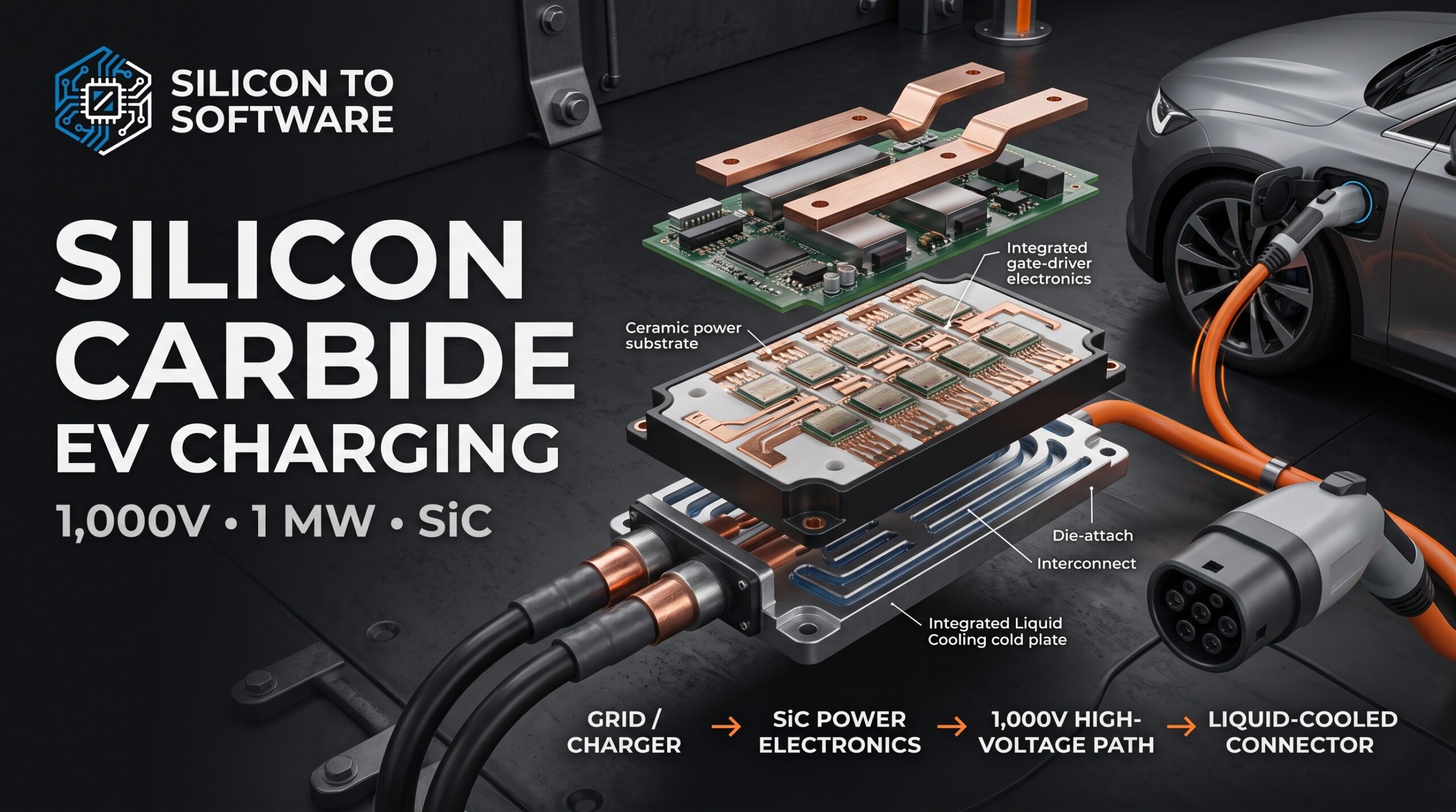
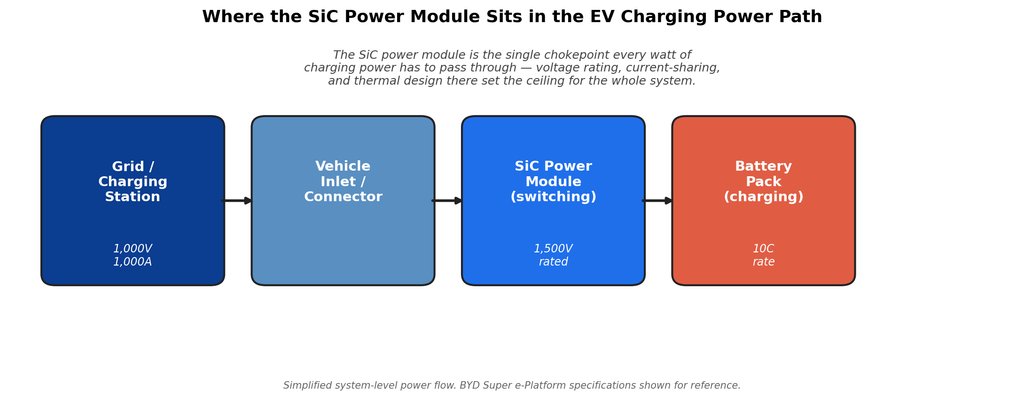
According to BYD’s official launch materials, the Super e-Platform launched March 17, 2025, in Shenzhen, running a full-domain 1,000-volt architecture, charging at up to 1,000 amps and a 10C rate, and pairing it with a self-developed SiC power chip rated to 1,500 volts. BYD states this is the highest voltage rating for an automotive-grade SiC chip in mass-production vehicle use.
Two things are worth separating here, since the original announcement compresses them into one headline figure. First, the device voltage rating (1,500V) is not the same as the system’s nominal operating voltage (1,000V) — a blocking-voltage margin above nominal bus voltage is standard automotive power-electronics practice, providing headroom against transient overvoltage during switching. Second, the 1,000A/1,000kW figures describe the charging system and battery’s rated capability, not a claim that a single semiconductor die carries the full 1,000A — real automotive power modules split current across multiple paralleled dies, bridge legs, and busbars, a point this piece returns to in the packaging section below.
BYD’s voltage-rating superlative is also narrower than it sounds. Wolfspeed sells automotive-qualified SiC MOSFETs rated to 1,700V, with its broader industrial product portfolio extending to a 2,300V class; 1,700V-class SiC devices are also available from multiple other suppliers, though not all such catalog parts are automotive-qualified — ROHM, for instance, offers a 1,700V SiC MOSFET explicitly marketed as a standard-grade, not automotive-grade, product. No source found confirms any higher-rated automotive-qualified SiC part deployed in a shipping production vehicle at volume, so BYD’s claim about its production-car deployment isn’t contradicted by anything found here — though that’s a narrower statement than “no higher-voltage automotive SiC device exists,” which would overstate what’s actually established.
BYD’s own materials state that battery packs draw roughly 600 kilowatts even near 90% state of charge — a flatter curve than most fast-charging systems manage well before that point. This figure is explicitly a company-reported test result, not independent instrumented measurement: trade coverage repeating it (Electronic Design) attributes it directly to BYD verbatim — “according to the company, tests have shown” — rather than describing its own test rig.
Press-release numbers and field behavior don’t always match, either. A livestreamed third-party charging test in 2026 recorded a peak localized external sensor reading of 76.42°C at the battery cell surface, while the vehicle’s own battery management system (BMS), read via OBD during the same session, reported a maximum pole temperature of 71°C — a 6.5°C spread was also recorded across different internal sensor positions (69.89–76.42°C). That gap illustrates a real, general measurement-precision point: localized external readings and system-level BMS reporting are not interchangeable, and neither figure alone constitutes a full picture of the pack’s thermal state. That single test doesn’t overturn the engineering case made here, but it’s a reminder that the packaging-versus-datasheet gap discussed later in this piece applies to the battery pack as much as it applies to the power module.
None of this moves through the vehicle without power modules built from switching devices with sufficient blocking-voltage margin, current-sharing capability, and thermal performance for a roughly 1,000-volt, megawatt-class powertrain. That’s the engineering story. The battery is the other half of it.
Why SiC Wins at High Voltage and Power Density
Every power semiconductor — the MOSFETs and diodes that switch high voltage on and off thousands or millions of times per second in an inverter or charger — has to survive the electric field that builds up across it while blocking voltage. Push that field past the material’s breakdown point and the device risks avalanche breakdown — a failure mode some devices are designed to briefly tolerate within a rated avalanche energy margin, but one that causes permanent damage outside that margin.
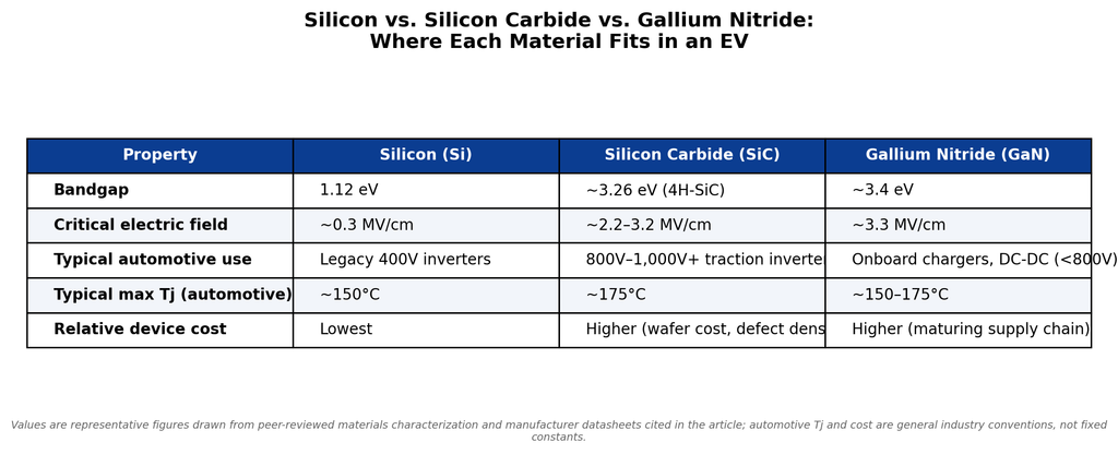
To be clear about what SiC actually solves: silicon is not physically incapable of blocking 1,200V or higher. Silicon IGBTs have operated for decades at these voltage classes in industrial drives, rail traction, and renewable-energy converters. What SiC changes is the combination of conduction loss, switching loss, switching frequency, power density, and cooling requirement achievable at a given voltage class — not whether the voltage can be blocked at all.
Silicon carbide’s critical electric field — the field strength it can sustain before breakdown — runs roughly an order of magnitude higher than silicon’s. Peer-reviewed materials characterization puts 4H-SiC’s bandgap at approximately 3.26 eV against silicon’s 1.12 eV, with a critical electric field around 2.2–3.2 MV/cm for 4H-SiC versus roughly 0.3 MV/cm for silicon. The material itself has been demonstrated in harsh-environment research devices operating up to roughly 600°C — but that figure describes a materials-science demonstration under research conditions, not a benchmark comparable to production automotive power-module operating limits, which are governed by packaging, die-attach, and interconnect reliability rather than the semiconductor material alone. The 175°C automotive junction-temperature figures discussed later in this piece belong to that separate, packaging-constrained category.
That electric-field gap matters because of what it lets a device designer do with drift-region thickness. To block a given voltage, silicon needs a thick, lightly doped drift layer to spread the electric field out before it reaches critical value. SiC, tolerating a much higher field before breaking down, can block the same voltage with a drift layer a fraction as thick. A thinner drift layer means lower on-resistance for a given breakdown voltage rating, in a smaller die — which is what translates into SiC’s real advantage: lower losses and higher power density at a given voltage and switching frequency, not an ability silicon categorically lacks.
None of this is free. SiC wafers have historically cost more to produce than silicon and carried higher crystal defect density, affecting usable die yield — general industry knowledge reflected across power-electronics trade coverage, though no specific current cost multiplier or yield figure is cited here. That premium is why SiC isn’t used everywhere silicon is used — it shows up where the voltage and switching-frequency requirements make the efficiency and density gain worth paying for. Automotive traction inverters and onboard chargers at 800V and above are exactly that case. The Model 3, launched in 2018, was among the earliest mass-production vehicles to carry a full-SiC traction inverter, using MOSFETs from STMicroelectronics — confirmed by independent teardown analysis, not just company messaging.
SiC isn’t the only wide-bandgap material in this picture. Gallium nitride (GaN) has seen real automotive adoption in a different part of the system — onboard chargers and DC-DC conversion, typically in the sub-650V-to-800V range, where its higher switching frequency and smaller passive components suit the lower-power AC charging path. Changan’s Qiyuan E07 is reported as an early commercial GaN OBC deployment. Today SiC and GaN occupy largely different primary sweet spots in a vehicle — but those boundaries are not fixed: GaN development is actively extending toward higher-power automotive applications, so the division of labor described here reflects current practice, not a permanent technical ceiling.
Voltage Is the Primary Engineering Lever
Go back to the cable problem. Power delivered is current multiplied by voltage: P = IV. If you want to deliver more power without proportionally increasing current — and therefore without proportionally increasing I²R heating in every conductor between the charger and the battery — raising system voltage is the most effective lever available, though not the only one available in principle. Larger or parallel conductors, improved contact and busbar design, and more aggressive liquid cooling can also raise permissible current, and BYD’s own architecture in fact raises both voltage and current together (to roughly 1,000V and 1,000A) rather than solving the problem through voltage alone. But raising voltage is what lets an OEM scale deliverable power without a proportional current increase and its associated conductor, connector, and cooling costs — which is why it’s been the dominant industry lever.
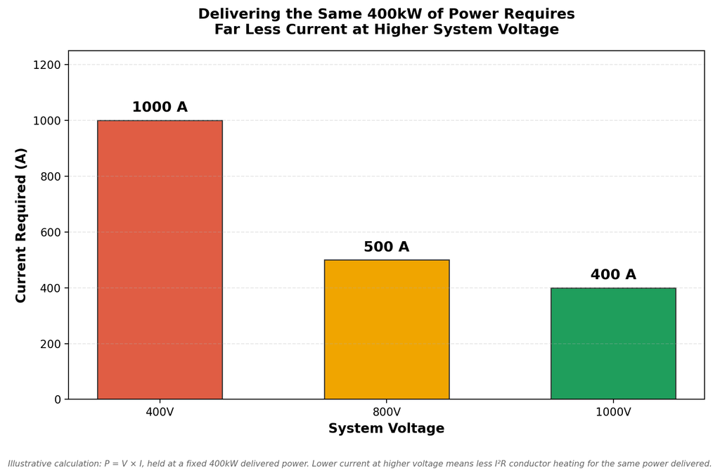
This is why the industry moved from 400V vehicle architectures toward 800V and now, with BYD, toward 1,000V. The trade-off runs the other direction through the rest of the vehicle: a higher-voltage architecture demands higher-voltage-rated components throughout the powertrain — insulation systems, isolation barriers, connector creepage and clearance distances — all requalified for the new voltage class. This is not a firmware update. It’s a system-wide redesign, and at megawatt power levels current remains a first-order design constraint in its own right: connector and busbar thermal design, contact resistance, and current-sharing across paralleled devices are not solved simply because system voltage went up.
None of this happens in isolation from the standards and safety framework governing how a vehicle and a charger negotiate that power in the first place. IEC 61851-23:2023 specifically addresses DC EV supply equipment and energy transfer requirements for DC fast charging, while IEC 61851-24:2023 covers the digital communication protocol used to control DC charging; the ISO 15118 family layers higher-level vehicle-to-charger authentication and communication — including Plug and Charge — on top of that. In North America, UL 2202 covers DC charging equipment safety (currently Edition 3, scoped to inputs up to 1,500V DC / 1,000V AC) and UL 2231-1/-2 covers personnel protection against shock. A 1,000V, megawatt-class system operates within that framework, not around it — though whether a given edition of any of these standards is legally mandatory depends on jurisdiction, certification scheme, and how it’s been incorporated into local law or OEM requirements.
Inside the Power Module: Thermal, EMI, and Short-Circuit Constraints
A SiC MOSFET’s datasheet numbers come from a test jig with a short, low-inductance switching loop. Put that same die into a real power module — bonded to a substrate, wired or sintered into a package, mounted to a cold plate, and paralleled with other dies to share current — and several things change.
Thermal Design
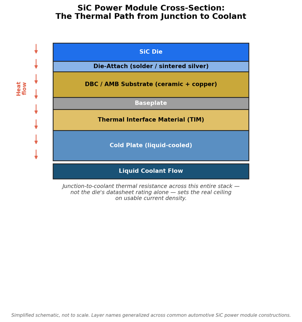
Automotive-grade SiC MOSFETs are commonly specified to a 175°C maximum junction temperature — a convention reflected across datasheets from suppliers including Infineon and Wolfspeed — and that rating gets validated through AEC-Q101 stress testing, though the standard itself doesn’t mandate 175°C as a fixed ceiling; it’s a manufacturer specification choice, tested against. In practice, sustained operation near that datasheet maximum accelerates thermally driven fatigue mechanisms in the package — CTE mismatch between die, die-attach, and substrate can drive delamination and interconnect fatigue over a vehicle’s power-cycling lifetime — so automotive power-electronics design typically targets operating margins below the datasheet ceiling rather than running continuously against it.
That headroom only matters if the thermal path from junction to coolant — die-attach material, substrate, thermal interface material, cold plate — can actually move heat out fast enough. Junction-to-coolant thermal resistance, not the device’s theoretical rating, sets the real ceiling on how much current density you can run through a given module footprint.
It’s also worth being precise about what AEC-Q101 actually covers: it’s a discrete-semiconductor qualification standard, not a complete power-module qualification framework. The automotive power-electronics industry uses a separate guideline — AQG 324, maintained by the European Center for Power Electronics (ECPE), now in its Release 04.1/2025 with a dedicated SiC annex — specifically for module-level and assembly-level qualification: thermal cycling, power cycling, and lifetime testing of the complete module, not just the bare die. Component-level qualification, module-level qualification, and full vehicle-system validation are three distinct steps, and conflating them understates how much validation work sits between a qualified die and a qualified vehicle.
EMI and Switching Loop Design
Switching speed carries its own liability: high dV/dt and di/dt edges couple through every parasitic inductance in the commutation loop — bond wires, substrate trace geometry, busbar routing. That coupling shows up as ringing and EMI, and can drive parasitic turn-on of a device that’s supposed to be off. Infineon’s own CoolSiC application literature documents this design challenge directly. Managing it requires active gate driver design and a commutation loop laid out for minimum inductance. A straight silicon-to-SiC substitution in an existing module layout, without addressing loop inductance and gate drive, can produce worse EMI performance than the silicon design it replaced.
Short-Circuit Ruggedness
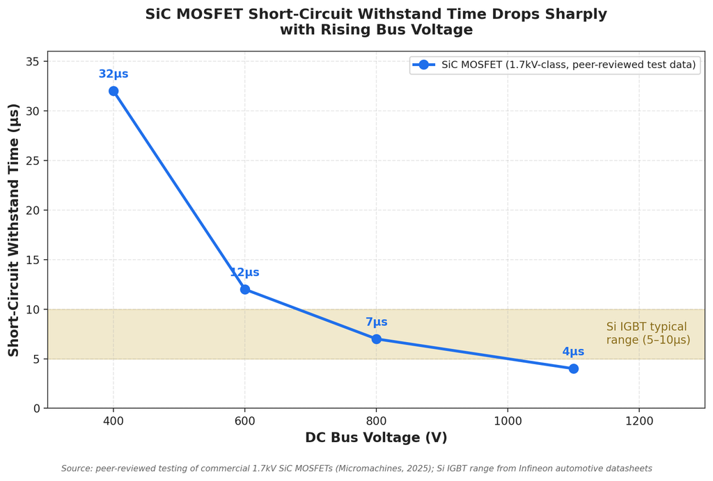
This is a trade-off the SiC-vs-silicon comparison usually skips. Silicon IGBT datasheets specify short-circuit withstand times in the same general order of magnitude as SiC MOSFETs, not the wide gap sometimes claimed: primary manufacturer datasheets and application notes from Infineon commonly show Si IGBT tsc figures around 5–10 microseconds under standard test conditions. SiC MOSFETs run shorter still — peer-reviewed measurement and Wolfspeed’s own short-circuit application note put representative SiC MOSFET withstand time at roughly 2 to 7 microseconds under manufacturer test conditions, driven by the same smaller die size and lower thermal capacitance that make SiC attractive in the first place.
This figure is bus-voltage dependent, and the relationship is well documented: peer-reviewed testing of commercial 1.7kV-class SiC MOSFETs found short-circuit withstand time dropping from roughly 32 microseconds at a 400V bus to roughly 4 microseconds at 1,100V, with intermediate readings of roughly 12 microseconds at 600V and roughly 7 microseconds at 800V. A device operating near the top of an 800–1,000V bus should therefore be expected toward the shorter end of the commonly cited 2–7µs range for automotive-class devices, not treated as sitting at a fixed midpoint.
Wolfspeed’s own application literature documents the same trend on a different device: one part they characterize drops from roughly 9µs at 400V bus to roughly 1.8µs at 800V. The real design consequence is that gate driver desaturation-detection circuits for either device family have to respond within a single-digit-microsecond window — SiC tightens that window further, and higher bus voltage tightens it more, but this doesn’t create an entirely new category of problem the way a “seconds versus microseconds” framing would suggest.
Automotive qualification of SiC power modules — against AEC-Q101 at the discrete-device level and AQG 324 at the module and assembly level — took years, not because the material was new, but because the full package had to prove it could survive a vehicle duty cycle.
Merchant Supply vs. Vertical Integration: Who’s Building the Chips
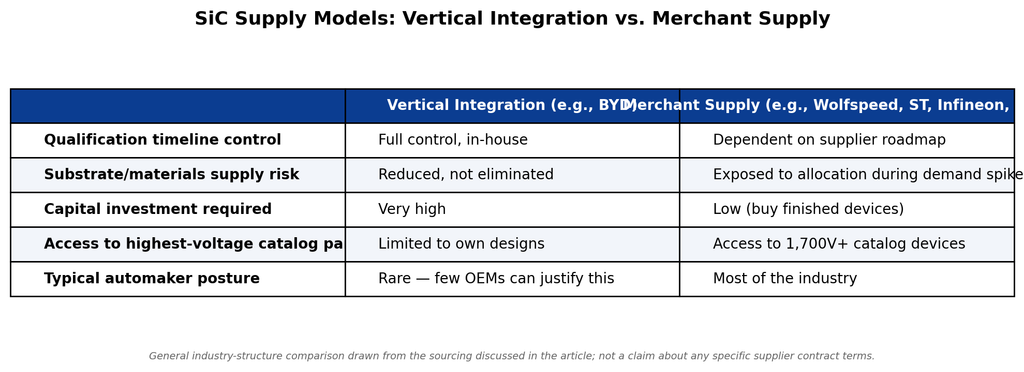
Two supply models are running in parallel here, and which one an automaker uses shapes what it can promise a customer.
BYD states its SiC power chips are self-developed and mass-produced, and independent industry reporting indicates this extends to genuine in-house manufacturing capacity — BYD’s Ningbo semiconductor operation and reported wafer fabrication capability go beyond chip design and final assembly alone. A secondary industry report describes a planned SiC wafer line at that facility targeting roughly 20,000 wafers/month once complete, though this specific capacity figure comes from trade reporting rather than a primary BYD capacity filing and should be read as a planned, not confirmed-operational, figure. BYD has also separately been reported to have taken an investment stake in an external SiC epitaxial-wafer supplier, TYSiC — suggesting a mixed model of owned facilities plus supplier investment rather than one clean category.
Most of the rest of the industry relies on merchant suppliers instead — Wolfspeed, STMicroelectronics, Infineon, onsemi, ROHM. Wolfspeed’s Mohawk Valley facility in Marcy, New York, which the company describes as the industry’s first purpose-built, fully automated 200mm SiC fab, opened in April 2022 as part of a broader industry shift to larger wafer diameters to improve device economics. As with BYD’s voltage-rating superlative discussed earlier, this “industry first” framing is Wolfspeed’s own characterization and wasn’t independently cross-checked here against competing 200mm SiC fab claims from other suppliers.
Vertical integration gives BYD more direct control over its own device development, qualification timeline, and capacity planning, though it does not necessarily eliminate all upstream exposure to SiC materials supply constraints. The merchant model gives other automakers access to comparable device physics without BYD’s capital commitment, at the cost of sitting in an allocation queue when demand spikes — and, notably, access to devices already rated at higher voltages than BYD has deployed in a shipping vehicle. Most automakers currently rely substantially on that merchant supply model rather than replicating BYD’s vertical integration.
The Battery’s Half of the Equation
A 10C charge rate isn’t survivable without cell-level engineering that suppresses lithium plating and other high-rate degradation and thermal mechanisms at the anode. Plating specifically happens when the anode’s electrochemical potential drops below 0V relative to lithium metal under high charging current — instead of intercalating normally into the graphite structure, lithium deposits as metal on the anode surface.
Peer-reviewed research on fast-charging failure mechanisms is specific about what plating costs: irreversible loss of lithium inventory, degraded active anode material, and in severe cases dendrite formation that can cause internal short circuits — the same underlying failure mode, incidentally, that solid-state battery designs have to engineer around too, just through a rigid rather than liquid electrolyte. It’s one of several failure modes every fast-charging battery design has to engineer around — alongside electrolyte transport limits, ohmic heating, and cathode-side degradation at high rates — and it’s why “10C” isn’t just a marketing number; it’s a claim about how well a cell suppresses this whole family of high-rate failure mechanisms.
According to BYD’s official announcement, the flash-charging Blade battery reduces internal resistance by 50% through “ultra-fast ion channels” built from positive to negative electrode — a design approach consistent with the industry’s general strategy for suppressing plating, which centers on improving ion transport so lithium intercalates fast enough that it never has the chance to plate. The specific resistance figure and mechanism are company-stated and not independently verified outside BYD’s own disclosure.
SiC and the battery are co-equal, necessary parts of this system, not a hierarchy. SiC removed a power-delivery bottleneck that would have made a 10C-capable cell irrelevant — there would be nowhere to safely route that much power without it. The cell removed a plating-and-thermal bottleneck that would have made SiC’s power-handling capability moot — a converter capable of a megawatt has nothing useful to do if the pack behind it can’t accept that rate without degrading or venting. Neither one alone produces a five-minute charge.
The Next Bottleneck: Grid Interconnects — Among Several Real Constraints
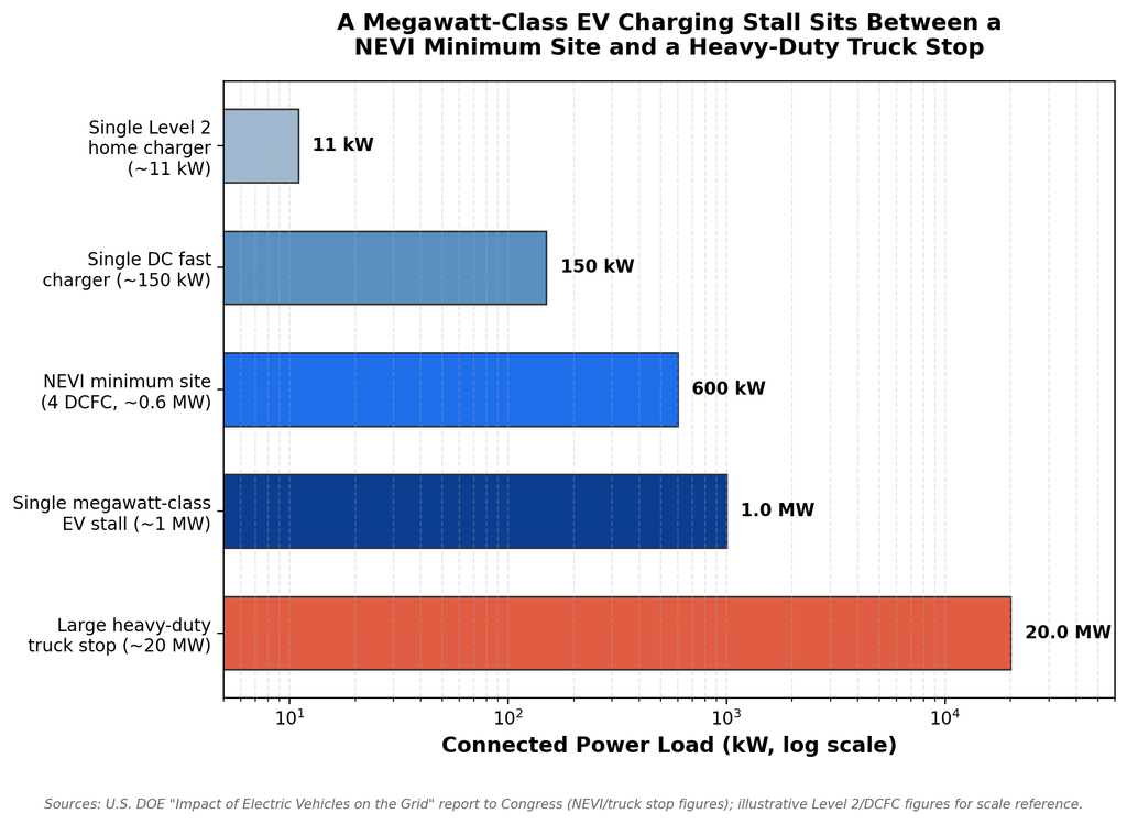
A single megawatt-class charging stall isn’t a small load by grid standards. A peer-reviewed NREL study modeling DC fast-charging stations sited behind a big-box retail grocery store’s meter — using charger power levels up to 350kW per port, still below BYD’s megawatt-class terminals — found that a station “has the potential to dwarf a big box building’s power demand if behind the same meter, increasing monthly peak power demand at the site by over 250%,” with cold-climate sites paired with demand-charge rate structures most exposed to the effect. A megawatt-class installation would be expected to strain a comparable connection further, though that specific figure describes the modeled retail-store scenario, not a BYD terminal directly.
For a closer order-of-magnitude anchor at BYD’s actual power level, a U.S. Department of Energy report to Congress notes that a charging site meeting the NEVI minimum of four DC fast chargers represents roughly 0.6 megawatts of connected charging power, while a large heavy-duty truck stop can require nearly 20 megawatts — putting a single megawatt-class passenger-vehicle stall in the same order of magnitude as several conventional fast chargers operating simultaneously.
BYD’s own megawatt terminals, per the company’s original March 2025 announcement, pair liquid cooling with an integrated energy storage buffer specifically to absorb that spike rather than pulling it directly off the grid. That announcement stated plans to build more than 4,000 such stations in China — a figure that is now stale: as of late August 2026, BYD has reported roughly 10,000 second-generation Flash Charging stations installed (a separate, higher-power 1,500kW-class rollout announced March 2026, distinct from the original 1,000kW Super e-Platform terminals this piece otherwise describes), with a stated target of 20,000 by year-end 2026, deployed partly through a partnership with Sinopec’s existing fueling-station network. The pace and scale of that rollout is itself a live, company-reported figure rather than an independently audited station inventory or a settled endpoint, and this piece’s original March 2025 sourcing predates it.
Grid interconnect capacity is a genuine and increasingly binding constraint on how fast this scales — but it isn’t the only one still in play. Cell-level thermal margins under sustained high-rate charging remain an active engineering question, as the 2026 field temperature data discussed earlier illustrates; connector and contact heating at sustained near-megawatt current, charging-curve behavior at high state of charge across ambient conditions, and site-level utilization economics for stationary buffer storage are all still-open parts of this system, not solved problems sitting behind a single grid bottleneck.
The vehicle-side power electronics problem — silicon’s practical efficiency and density limits at this voltage and current combination — has a demonstrated engineering answer in SiC. Grid connection and site power capacity are becoming an increasingly prominent constraint on top of that — a strain on grid infrastructure from a new class of megawatt-scale load that shows up in AI data center power demand as much as EV charging, even though the two problems have little else in common. That’s this author’s engineering read of where the evidence currently points, not a claim that every other constraint in this system has been resolved.
What This Piece Doesn’t Cover
A megawatt-class charging system also raises real cybersecurity and functional-safety questions, and it’s worth being precise about where each standard’s scope actually sits rather than treating them as a blanket answer. On the vehicle side, ISO/SAE 21434 addresses cybersecurity engineering for road-vehicle electrical and electronic systems and their interfaces, while ISO 26262 addresses functional safety for safety-related vehicle E/E systems.
Vehicle-side charging control — high-voltage contactor control, isolation monitoring, authentication, and charger communication as they touch the vehicle’s own systems — can fall within those engineering processes, and functions like vehicle-side HV contactor control are the kind that typically receive ASIL-based treatment in real automotive functional-safety programs. But the charging station itself, the OCPP backend, and the broader supporting network infrastructure introduce additional cybersecurity and safety domains that sit outside the scope of either standard alone.
Neither ISO 26262 nor ISO/SAE 21434 is addressed in any technical depth in this piece; a full system-level treatment of a megawatt-class, digitally authenticated charging platform’s safety and security architecture — spanning both the vehicle and the charging infrastructure — is outside what this article set out to explain. The charging-port attack surface specifically isn’t theoretical, either — documented research has already demonstrated exploitable vulnerabilities in real charging hardware and the V2G communication stack, a separate story from the power electronics covered here.
Quick Answer: Is SiC Used in Every EV?
No. SiC shows up specifically where 800V-plus system voltage and high switching frequency make its cost premium worth paying — primarily traction inverters and DC fast-charging power paths in higher-voltage platforms. Many EVs, particularly 400V-architecture vehicles, still use silicon IGBTs in their main inverter, and even 800V+ platforms often mix SiC in the traction inverter with GaN or silicon in lower-power subsystems like the onboard charger. There’s no single answer that applies across the whole EV market — silicon carbide EV charging capability is a per-subsystem, per-voltage-class engineering decision, not a blanket material choice.
About the Author
Imran Valiani | Sales Director, PCB Electronics Manufacturing
20+ years working with major Bay Area and global tech clients. Founder of Silicon to Software, where I write about the hardware layer — PCB fab, AI gear, autonomous systems, and cyber — the stuff most tech writers have never touched. Literally.
Follow: X @SiToSoftware | LinkedIn
This article was developed with AI assistance and edited, fact-checked, and reviewed by the author. See my full AI disclosure.
Sources
Company / primary announcement
- BYD — “BYD Unveils Super e-Platform with Megawatt Flash Charging for Electric Vehicles, Matching Refueling Speeds”, byd.com, March 17, 2025
- BYD — “BYD breaks down final barriers to electrification with Blade Battery 2.0 and FLASH Charging”, media.byd.com, March 2026
Trade / secondary reporting
- Electronic Design — “Tests Show BYD Battery Packs Draw 600 kW at 90% State of Charge”, March 27, 2025
- CarNewsChina — “BYD Flash Charging blind spot: 76°C hotspot vs 71°C BMS, 6.5°C thermal gap”, May 21, 2026
- CarNewsChina — “BYD hits 10,000 Flash Charging Stations, targets 20,000 in 2026 with China’s oil giant Sinopec”, August 27, 2026
- CarNewsChina — “BYD hits 10,000 Flash Charging stations in 6 months with 1.83M users and 33% non-BYD”, August 28, 2026
- SLKOR — “BYD Builds World’s Largest Silicon Carbide (SiC) Plant” (secondary report on BYD’s Ningbo SiC wafer capacity — planned figure, not primary-confirmed)
- S&P Global AutoTechInsight — “BYD invests in semiconductor technology company TYSiC”
- ElektronikNet — “Automotive is Driving SiC Adoption” (System Plus/Yole Tesla Model 3 SiC inverter teardown coverage)
- Navitas Semiconductor — “Navitas Announces Plans for 200mm GaN Production with PSMC” (Changan GaN OBC context)
Manufacturer datasheets/application notes
- Wolfspeed — E3M0900170J, 1700V automotive-qualified SiC MOSFET, product page
- Wolfspeed — Bare Die Silicon Carbide (SiC) MOSFETs product catalog (2,300V industrial-class devices)
- Wolfspeed — PRD-08296: SiC MOSFET Short Circuit Application Note
- ROHM — SCT2750NWCTL1 product page (1,700V SiC MOSFET, standard-grade — not automotive-qualified)
- Infineon — CoolSiC 1200V G2 MOSFET application note
- Infineon — AIKQ120N75CP2 automotive IGBT datasheet
Peer-reviewed research
- Wang et al., “Short-Circuit Performance Analysis of Commercial 1.7 kV SiC MOSFETs Under Varying Electrical Stress”, Micromachines, 2025; also indexed at PubMed
- “Study of 4H–SiC trench MOSFET structures”, Solid-State Electronics, ScienceDirect (4H-SiC bandgap and critical electric field values)
- “Challenges in SiC power MOSFET design”, Solid-State Electronics, ScienceDirect
- Gilleran, M., Bonnema, E., Woods, J., et al., “Impact of electric vehicle charging on the power demand of retail buildings”, Advances in Applied Energy 4 (2021), 100062 — NREL-authored study (source of the >250% peak-demand figure)
- Kyoto University — “A transistor that operates at 600°C”, research news, August 24, 2026
Government/standards documentation
- U.S. Department of Energy — “Impact of Electric Vehicles on the Grid,” report to Congress, October 2024
- IEC 61851-23:2023 — DC EV supply equipment
- IEC 61851-24:2023 — Digital communication for control of DC EV charging
- ISO 15118-20:2022 — Vehicle to grid communication interface
- ISO/SAE 21434:2021 — Road vehicles, cybersecurity engineering
- ISO 26262-1:2018 — Road vehicles, functional safety, vocabulary
- UL 2202 — DC charging equipment for electric vehicles, Edition 3
- UL 2231-1 — Personnel protection systems for EV supply circuits
- AEC-Q101 Rev-D — Failure Mechanism Based Stress Test Qualification for Discrete Semiconductors, Automotive Electronics Council
- ECPE — AQG 324, Automotive Power Module Qualification Guideline, European Center for Power Electronics