
Printed Electronics vs. Flexible PCB: What Conductive Ink Can and Can’t Replace
Conductive inks and additive manufacturing are opening up substrates and geometries that rigid FR-4 and even standard flex-PCB processes were never built to reach — but the sintering step still decides where this technology stops.
Table of Contents
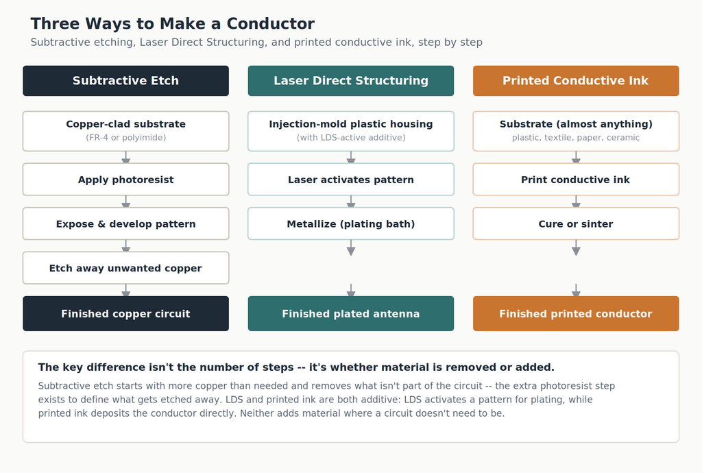
For most of the history of printed circuit board manufacturing, making a board has meant starting with more copper than you need and etching away everything you don’t want. You laminate copper foil to a substrate, apply a resist, expose it, develop it, and dissolve everything the resist didn’t protect. What’s left is your circuit. It’s a subtractive process, and it has worked well enough, for long enough, that most engineers never think about the fact that it’s fundamentally wasteful — you’re throwing away copper to define a shape.
Printed electronics inverts that logic. You start with nothing and add exactly the conductor you need, layer by layer, sometimes with an inkjet head that looks like it belongs in an office printer rather than a fab.
The part that doesn’t make it into the marketing copy is the step that decides whether any of it works: sintering. You can print a perfect conductive pattern with a conductive ink — silver nanoparticle, copper nanoparticle, or carbon-based — and have it measure as effectively non-conductive until the particles are fused together into a continuous conductive path. That fusion step typically requires heat.
The amount of heat required to get good conductivity is often more than the low-cost, flexible substrate you chose printed electronics to take advantage of can actually survive.
This piece breaks down what printed electronics actually is versus what it gets confused with, the specific materials tradeoff that caps its performance, where it’s already qualified for production, where the “printed electronics enabled foldable phones” narrative gets the engineering wrong, and the reliability constraint that will determine whether the technology ever expands beyond its current footprint.
What Printed Electronics Actually Is (and Isn’t)
The trade press has a habit of using “printed electronics,” “flexible circuits,” and “additive manufacturing” as if they were interchangeable. They aren’t, and the distinction matters for anyone specifying a design.
A flexible printed circuit (FPC) is still a conventional copper process — subtractive or semi-additive — typically built on a polyimide substrate, though lower-cost PET-based flex constructions exist for less demanding applications. It’s flexible because the substrate and the thin copper layer can bend, not because the manufacturing process is fundamentally different from a rigid board. FPCs are qualified under IPC-6013 (the current published revision is IPC-6013E; a further revision, IPC-6013F, appears to be in development as of this writing but had not been published), the dedicated specification for flexible and rigid-flex printed boards, which — like IPC-6012 for rigid boards — applies the three performance classes (Class 1, 2, and 3) defined in IPC-6011, the generic performance specification both documents build on. Those classes are based on the required level of performance and acceptance criteria for the intended service conditions, not on industry vertical by itself — a medical device isn’t automatically Class 3, and aerospace isn’t synonymous with one specific class; specialized sectors often layer additional customer-specific or addenda requirements on top of the base class. Satellite electronics, for instance, run under IPC-6012 Class 3 plus a NASA-specific space addendum that goes well beyond the base standard — the same layering logic that applies wherever IPC-6013 gets specified for a flex or rigid-flex build.
Printed electronics is a different animal. It’s the direct deposition of a conductive ink — via inkjet, screen printing, or aerosol jet — onto substrates that were never designed to be copper-clad at all: PET, textiles, ceramics, injection-molded plastics, even paper. Inkjet and aerosol jet are maskless, digitally-driven processes; screen printing still requires a physical screen or stencil per design, closer in that respect to a masked process, though all three add material rather than remove it. There’s no etching. There’s no copper foil lamination. The conductor is built up from a liquid or paste, then cured or sintered to become electrically continuous — the exact mechanism depends on the ink: metal nanoparticle inks are sintered (fused via heat into a continuous metallic structure), while carbon-based and polymer-bound inks are typically cured rather than sintered, conducting through particle-to-particle contact within a binder instead. The rest of this piece focuses on the metal nanoparticle systems, since that’s where the conductivity-vs-copper comparison and most of the reliability data exist.
That distinction is why an engineer evaluating “printed electronics” as an option needs to ask which deposition method and which ink chemistry a vendor is actually using, rather than treating it as one undifferentiated category of technology.
The Conductivity-Flexibility-Cure Temperature Triangle
You cannot simultaneously maximize conductivity, flexibility, and low-temperature processing with the ink systems available today. Push on one, and you give something up on another — and this is the tradeoff most coverage of printed electronics skips entirely.
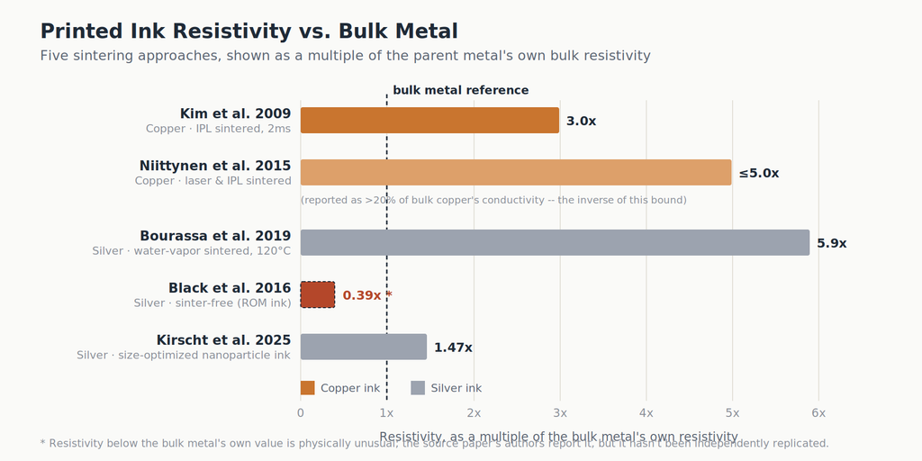
The conductivity gap between printed ink and bulk copper is real and well documented. Kim et al. (2009) found that intense pulsed light sintering of a copper nanoparticle ink produced a resistivity of 5 microohm-cm — roughly three times that of bulk copper — without damaging the underlying polymer substrate. A separate, later study by Niittynen et al. (2015) using both laser and intense-pulsed-light sintering independently corroborated a similar magnitude, achieving conductivities exceeding 20 percent of bulk copper’s conductivity.
On the silver side, water-vapor-assisted thermal sintering of a silver nanoparticle ink at 120°C for 30 minutes produced resistivity nearly six times that of bulk silver, while a sinter-free silver ink process reported a resistivity as low as 39.2 percent of bulk silver’s own resistivity — an unusually strong result, consistent across every independent citation of that paper’s abstract, but one that would benefit from independent replication before being treated as representative. “Sinter-free” here means the process eliminates a separate post-deposition sintering step, not thermal input altogether — the ink was still printed with the substrate held at roughly 110-120°C during deposition. The most recent figure in this comparison comes from a November 2025 study using a synthesis approach that decouples silver nanoparticle size from organic binder content: the best-performing formulation reached a resistivity of 2.34 microohm-cm, roughly 68 percent of bulk silver’s conductivity — the strongest result cited here, and recent enough that it likely represents close to the current state of the art rather than a dated snapshot. These are legitimate engineering results, each the product of a specific ink chemistry and cure method. But most of them are still meaningfully short of copper, and that gap is exactly what a design has to account for if it’s carrying any meaningful current rather than a low-current sensor signal.
The reason the gap exists comes down to sintering physics. Metal nanoparticle inks arrive as discrete particles suspended in a carrier, and closing the resistivity gap between those printed particles and their bulk metal counterpart has been a persistent, actively studied challenge across the field, because conductivity depends on how completely the particles fuse into a continuous metallic structure — and more complete fusion generally means more thermal energy. Higher sintering temperatures push conductivity closer to bulk values. They also push you further away from what a lot of interesting low-cost substrates — PET foremost among them — can survive without deforming or degrading.
This is why alternative sintering methods — photonic, UV, plasma, and microwave sintering — exist. They’re not an incremental refinement; they’re an attempt to break the temperature/conductivity coupling by delivering energy to the ink layer without heating the bulk substrate. Each comes with its own equipment cost, throughput limitation, or conductivity ceiling. There is no single ink-and-cure combination that is simultaneously the most conductive, the most flexible-substrate-compatible, and the cheapest to process. Every printed electronics design decision is a negotiation across those three variables, and treating it as a solved problem is where a lot of over-promised timelines come from.
Where Design-for-Manufacturability Meets This Tradeoff
For engineers coming from a rigid-board DFM background, the closest analog is laminate selection under competing electrical and thermal constraints — you’re used to trading dielectric loss for cost, or copper weight for etch tolerance, the same category of DFM discipline that quietly decides fabrication yield long before a board reaches qualification testing. This is the same category of decision, just with sintering temperature and substrate glass transition temperature as the competing variables instead of Dk and cost per panel.
Where It’s Already Production-Real
That tradeoff doesn’t strand printed electronics in the lab. It just draws a hard line around where the technology is actually mature today: applications that don’t demand copper-level conductivity or multilayer complexity.
Aerosol jet printing, in particular, was reportedly in volume production for conformal antennas as of the mid-2010s. Optomec’s aerosol jet process was used to print mobile device antennas — LTE, NFC, GPS, WiFi, WLAN, and Bluetooth — directly onto injection-molded plastic housings, and according to Optomec, RF testing by a cell phone component supplier showed antenna performance comparable to conventionally manufactured antennas, with machine throughput for a typical antenna pattern reported at around 30,000 units per week on a single system as of that disclosure.
Worth flagging: the conductivity figures elsewhere in this piece are bulk DC resistivity measurements, which aren’t the metric that governs antenna performance at RF — skin effect and surface roughness matter more there than bulk conductivity does. Whether that specific throughput and volume-production status still holds a decade later hasn’t been independently reconfirmed here. The same aerosol jet process has been extended to molded interconnect devices, conformal sensors for industrial and aerospace parts, and RFID-class applications — all of which share the same profile: low current, single or few conductive layers, and geometries that a rigid or even flexible copper-clad board can’t conform to.
That’s the maturity curve as it actually stands. Printed electronics wins today in applications where the requirement is “get a conductive path onto this 3D or unconventional surface,” not “replace a multilayer high-speed digital board.” The unglamorous stuff — antennas, in-mold sensors, disposable diagnostics — is where the process economics and the current ink capability actually line up.
It’s worth naming exactly who printed electronics is competing against for that 3D-antenna use case, because it isn’t a foregone win. Laser Direct Structuring (LDS) — a process where a laser activates a pattern on specially doped injection-molded plastic, which is then metalized by plating — is the more established incumbent for embedding antennas directly into a device housing. LPKF, the company behind the LDS process, states its antenna structures have been used “millions of times over” in cell phone housings — a real number, but a company-stated one, not an independently audited market-share figure. Printed ink and LDS are competing approaches to the same problem, each with its own cost and complexity tradeoffs; printed electronics hasn’t displaced the incumbent so much as carved out the applications where its lower tooling cost and digital design flexibility matter more than LDS’s plating precision and installed base.
Raw material cost is only one input into that comparison, and it would overstate the case to reduce it to “copper-based inks cost less.” Total unit cost depends on ink formulation, oxidation control, deposition passes, curing or sintering energy and throughput, yield, rework, and surface preparation — for printed processes — against resin, laser, and plating economics that are themselves highly scale-dependent for LDS. Printed deposition can plausibly reduce tooling and design-change costs in some geometries, while LDS benefits from an established industrial process chain; total cost is application- and volume-dependent, and no publicly available source puts an actual dollar-per-unit figure on the comparison. [SOURCE REQUIRED] for that number; this is a market with two viable manufacturing options, not one technology waiting to be crowned.
The Foldable Phone Myth
Consumer technology coverage overstates the case here more than anywhere else in this topic. Printed electronics gets credited, implicitly or explicitly, as the enabling technology behind foldable phones. It largely isn’t.
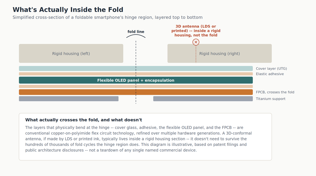
Commercial foldable architectures commonly use conventional FPC/FPCB structures across the folding or hinge region — not a printed conductive ink trace. Patent filings describing foldable device architectures consistently show the flexible display panel connected to the main board through an FPCB, with the flexible OLED panel itself handling the display function and the driving IC for the display mounted on that same flexible printed circuit. Those patents establish a disclosed architecture used by at least the filing manufacturer, not a confirmed bill-of-materials for every commercial foldable across every brand.
Separately, patent documentation on foldable phone electrical architecture describes dual mainboards connected across the hinge specifically by a flexible printed circuit, reflecting the standard architecture used across foldable phone designs from multiple manufacturers.
A role for printed electronics somewhere in a given foldable device’s bill of materials — an antenna or a sensor, for instance — isn’t ruled out by any of this. But the primary engineering achievement that makes the fold itself survivable is broader than any single component. Samsung Display’s own account of its Z Fold 7 panel, for instance, credits a 50 percent increase in outermost ultra-thin glass (UTG) thickness, a new high-elastic adhesive layer offering over four times the recovery performance of its predecessor, a new flattening structure to distribute shock evenly, and a titanium support plate — alongside flexible OLED materials, encapsulation, and conventional FPC interconnect. That’s a materials-and-mechanical-design story with several contributing layers, not a single breakthrough component. And even where a 3D-conformal antenna is needed elsewhere in the housing, LDS remains the more established manufacturing choice across the industry, which further narrows the plausible role printed electronics plays in any given foldable’s design. Whether any specific commercial foldable model uses printed conductive ink anywhere in its design is a claim that would still need verification against a component-level teardown of that specific device — that level of BOM-specific confirmation sits behind paid teardown services and isn’t publicly available.
Crediting printed electronics as the reason foldables work isn’t just imprecise — it points engineers and readers toward the wrong maturity curve entirely.
The Reliability Constraint Nobody’s Solved Yet
For dynamically flexing interconnect applications specifically — the kind a foldable phone or a hinge-crossing FPC has to survive — the constraint that actually decides how far printed electronics can expand isn’t conductivity. It’s mechanical fatigue life under repeated flexing. That’s a different question from resistivity, adhesion, oxidation resistance, or environmental aging, which matter more in other application classes; this section is about the dynamic-flex case specifically.
Flexible printed circuits have decades of field data behind their flex-cycle reliability, and Samsung’s publicly documented approach to foldable phone qualification reflects that maturity: the company has rated its foldable hinge and display assembly at 200,000 fold cycles since the Galaxy Z Fold 2, with the Z Fold 7 rated for up to 500,000 folds under company testing — a figure that assumes consistent temperature, fold angle, speed, and no external contaminants under laboratory conditions. That’s a system-level panel qualification figure, not a number assigned specifically to the FPC conductor crossing the hinge — worth keeping in mind before treating it as a precise denominator. Still, it’s the best public reference point for what a flex interconnect technology needs to survive in a shipping consumer foldable.
Printed conductive ink traces have historically lagged well behind that bar, and the literature shows real, if uneven, progress toward closing the gap. Reliability research on aerosol-jet-printed metallic sintered conductive patterns, citing work by Reboun et al. (2016), found bending endurance under 10,000 cycles, with visible cracking after that many cycles. A 2022 study of screen-printed polymer thick-film silver ink pushed that to 30,000 cycles with only a 2.64 percent resistance increase. A November 2025 study on silver nanoparticle ink — using a synthesis approach that decouples particle size from organic binder content — reported the best-performing formulation surviving 50,000 cycles at a 2.9mm bend radius with a 56.7 percent resistance increase and no noticeable defects observed by SEM at the bend location, alongside a resistivity of 2.34 microohm-cm, roughly 68 percent of bulk silver’s conductivity — the best conductivity figure in this piece by a wide margin.
That’s real, documented movement: roughly 10,000 to 30,000 to 50,000 cycles across 2016, 2022, and 2025. Against Samsung’s 200,000-to-500,000-cycle bar, the gap has narrowed from a 20x-to-50x shortfall to something closer to 4x-to-10x using the best 2025 figure — still a substantial gap, not a closed one, but a meaningfully different story than the 2016 baseline alone would suggest. One caveat worth stating plainly: none of these cross-study comparisons are fully apples-to-apples. Published bend-cycle studies vary in bend radius (commonly cited in the roughly 2 mm-to-10 mm range), strain, conductor thickness, substrate, failure criteria, and test frequency, and there’s no standardized methodology across the field for comparing them directly. Treat the multiples above as directional orientation, not a normalized fatigue-equivalence calculation.
Durability also isn’t uniform across ink chemistries and mechanisms. The aerosol-jet result is a sintered metallic film — rigid, diffusion-bonded nanoparticles with little tolerance for strain. The screen-printed result uses silver flakes suspended in a hyper-elastic polymer binder and cured rather than sintered — conductivity comes from flake-to-flake contact within a matrix that can flex with the substrate, not from a continuous metallic structure. The mechanism difference is likely a real part of why cured, binder-based systems tend to outperform rigid sintered films under strain, not just a formulation tweak on the same underlying process.
The mechanism matters at the microstructural level too. Peer-reviewed fatigue research using in-situ electron microscopy on cyclically strained silver nanoflake inks found that fatigue damage in these systems occurs primarily through the widening of cracks that form during the initial stretch, rather than new crack formation or delamination from the substrate as cycling continues, with crack depth and resistance growth varying by ink formulation and substrate. That failure mode is distinct from the ductile fatigue behavior engineers are used to characterizing in a rolled or electrodeposited copper foil on a flex circuit, and it means existing copper flex-fatigue models should not be assumed to transfer directly to printed ink systems without separate validation.
Ink and process performance has clearly improved over the past decade, and there’s no reason to assume that stops — new precursor chemistries and processing methods (photonic, plasma, and hybrid additive approaches) have produced non-incremental jumps before and could again. What hasn’t happened yet is closing the remaining 4x-to-10x cycle-life gap while also demonstrating it at the level of a complete, manufacturable interconnect system rather than a lab coupon — with the terminations, environmental exposure, and failure-mode characterization that a production part actually needs. That’s the harder, less glamorous problem, and it’s the one that actually gates whether this technology moves beyond antennas and sensors into higher-cycle-life, dynamically-flexing interconnect applications.

The Decision Engineers Actually Need to Make
This isn’t an argument against printed electronics. It’s an argument for treating it the way PCB engineers have always had to treat material and process selection: as a decision driven by what the specific application demands, not by what’s generating the most press coverage.
If the requirement is a conformal antenna on an injection-molded housing, or a low-current sensor on a substrate that can’t tolerate copper-clad processing, printed electronics is a mature, production-proven answer today. If the requirement is anything approaching foldable-phone-class dynamic flex-cycle life, or dense, controlled-impedance, current-carrying multilayer interconnect comparable to a production FPC or rigid PCB, conventional flex-PCB technology — qualified under IPC-6013, backed by decades of copper fatigue data — is still the right tool, and printed electronics isn’t there yet.
The interesting shift isn’t that you can print a circuit instead of etching one. It’s that engineers now have a legitimate additional column in the process-selection table, and the job is the same as it’s always been: match the interconnect technology to what the application actually requires, not to what looks the most novel on a data sheet.
Worth being explicit about what this piece hasn’t covered: yield and rework economics for defective printed traces, in-line test methodology for delicate ink conductors, and the regulatory/handling profile of nanoparticle inks (RoHS/REACH status, inhalation exposure during printing and curing) are all real factors in an actual process-selection decision, and none of them are addressed here. This piece is a materials-and-reliability framing, not a full manufacturing-readiness assessment — treat it as the first filter, not the last one.
About the Author
Imran Valiani | Sales Director, PCB Electronics Manufacturing
20+ years working with major Bay Area and global tech clients. Founder of Silicon to Software, where I write about the hardware layer — PCB fab, AI gear, autonomous systems, and cyber — the stuff most tech writers have never touched. Literally.
Follow: X @SiToSoftware | LinkedIn
This article was developed with AI assistance and edited, fact-checked, and reviewed by the author. See my full AI disclosure.
Sources
Peer-reviewed research
- Kim, H-S., Dhage, S.R., Shim, D-E., Hahn, H.T. “Intense pulsed light sintering of copper nanoink for printed electronics.” Applied Physics A 97, 791–798 (2009). DOI: 10.1007/s00339-009-5360-6
- Niittynen, J., Sowade, E., Kang, H., Baumann, R.R., Mäntysalo, M. “Comparison of laser and intense pulsed light sintering (IPL) for inkjet-printed copper nanoparticle layers.” Scientific Reports 5, 8832 (2015). DOI: 10.1038/srep08832
- Bourassa, J., Ramm, A., Feng, J.Q., Renn, M.J. “Water vapor-assisted sintering of silver nanoparticle inks for printed electronics.” SN Applied Sciences 1, 517 (2019). DOI: 10.1007/s42452-019-0542-0
- Black, K., Singh, J., Mehta, D., Sung, S., Sutcliffe, C.J., Chalker, P.R. “Silver Ink Formulations for Sinter-free Printing of Conductive Films.” Scientific Reports 6, 20814 (2016). DOI: 10.1038/srep20814
- “Smaller is better: reducing silver nanoparticle size without excess ligands enhances conductivity and flexibility in printed thin films.” npj Flexible Electronics (2025). DOI: 10.1038/s41528-025-00496-3
- Reboun, J., Pretl, S., Navratil, J., Hlina, J. “Bending endurance of printed conductive patterns on flexible substrates.” 2016 39th International Spring Seminar on Electronics Technology (ISSE), IEEE, pp. 184–188 (2016) — cited via Ali, M.A.A., Kay, R.W. “A review of aerosol jet printing — a non-traditional hybrid process for micro-manufacturing.” International Journal of Advanced Manufacturing Technology, DOI: 10.1007/s00170-019-03438-2
- Suhaimi, M.I., Nordin, A.N., Ralib, A.A.M., Voiculescu, I., Mak, W.C., Lim, L.M., Samsudin, Z. “Mechanical durability of screen-printed flexible silver traces for wearable devices.” Sensing and Bio-Sensing Research 38, 100537 (2022). DOI: 10.1016/j.sbsr.2022.100537
- Li, Q., Antoniou, A., Pierron, O.N. “In Situ Scanning Electron Microscopy Crack Characterization and Resistance Evolution in Cyclically-Strained Ag Nanoflake-Based Inks.” ACS Applied Nano Materials (2024). DOI: 10.1021/acsanm.4c05133
Standards
- IPC-6013E, “Qualification and Performance Specification for Flexible/Rigid-Flexible Printed Boards.” IPC/Global Electronics Association, September 2021. (IPC-6013F is reportedly in development but had not been published as of this writing.)
- IPC-6011, “Generic Performance Specification for Printed Boards” (source of the Class 1/2/3 performance-class definitions applied by IPC-6012 and IPC-6013).
Company technical documentation and press releases
- Optomec, “Advances in 3D Printed Electronics” and printed-antenna technical pages (optomec.com) — aerosol jet antenna throughput and RF-testing disclosures.
- Optomec aerosol jet application documentation — molded interconnect devices, conformal sensors, RFID.
- LPKF, “3D-MID Technology with Laser Direct Structuring (LDS)” (lpkf.com) — LDS process description and smartphone-antenna deployment claim.
- KYOCERA AVX and Taoglas LDS technical pages.
- Samsung Display, “Samsung Display’s Foldable OLED Panel Proves Exceptional Durability with 500,000-Fold Test,” July 22, 2025 (global.samsungdisplay.com/31384).
- Bureau Veritas, “Bureau Veritas verifies Samsung Display’s Industry-Leading Foldable OLED Durability,” July 31, 2025 (cps.bureauveritas.com).
- Oak Ridge National Laboratory, “Multi-layer Printing of Complex Antennas Using Aerosol Jet Technology” (DOE-funded CRADA final report, ornl.gov).
Patent filings
- US Patent documentation, “Foldable device” family (e.g., USPTO nos. 11567540, 12153472, 10901464, 10423196).
- Patent documentation, “Foldable display apparatus, manufacturing method therefor, and terminal device” (USPTO no. 12501797).
- LDS antenna manufacturing patent literature (e.g., USPTO nos. 8080995, 8659487, 10472536, 11469493).
A small number of figures in this piece — LDS smartphone market penetration and printed-electronics-vs-LDS cost comparisons — could not be traced to an audited primary source and are either omitted or explicitly flagged as unverified in the text.