Your Embedded Hardware Has a Quantum Problem Nobody Is Talking About
The chip in your car, your hospital’s infusion pump, your building’s security panel — may not be upgradeable. For a lot of deployed hardware, the path ends in physical replacement. Here’s the board-level reality nobody’s published yet.
Table of Contents
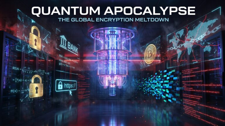
Post-quantum cryptography embedded systems have a problem the software world isn’t talking about — the algorithms don’t fit the hardware.
Let me start with the number that should end the “we’ll deal with it later” conversation.
489.9 milliseconds.
That’s the 99th-percentile signing time for ML-DSA-44 — the lowest-security post-quantum signature standard — on an ARM Cortex-M0+ running at 133 MHz (per arXiv:2603.19340, March 2026 preprint). If your system has a 100 ms hard real-time deadline — a lot of industrial control loops do — that’s not a slow migration. That’s a failed migration. The chip can’t do the job even at the lowest security level.
And that’s before we even get to whether it fits in RAM. It often doesn’t.
I think this is what most post-quantum cryptography embedded systems conversations miss entirely. Everyone’s focused on which algorithm to pick. The actual problem, in my experience, is whether your hardware can run it at all.
New to this? Start with [Part 1: The Quantum Computer Is Coming: Why Today’s Encryption Could Soon Be Useless] first. This piece is the hardware deep-dive.
Most quantum-encryption talk stays at the software layer. Change the algorithm. Patch the server. Ship it.
That works for cloud. It is dangerously wrong for most of the physical world.
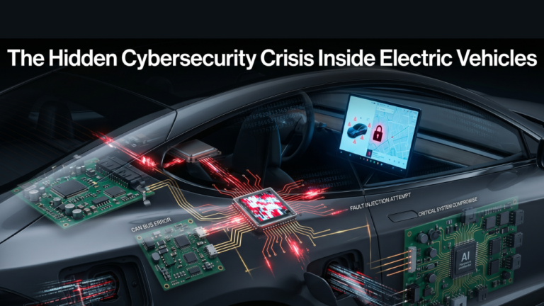
Think about what actually runs quietly around you. The chip managing keyless entry in your car. The controller in a hospital infusion pump. A security module in a power substation that nobody opens for five years. A smart meter on the side of your house. None of these get patched on a Tuesday. They’re physical objects — chips on boards — built for a world where the crypto they run was assumed to be safe forever.
That assumption is ending. For a big chunk of those devices, there’s no firmware update that fixes it. You hit silicon. For some, that means a new chip on a new board. For others, it means external secure element co-processors, gateway-assisted PQC termination, or documented risk acceptance while you wait out a replacement cycle.
None of those are fast. None are cheap.
I’ve had the meeting where someone from IT presents the NIST standards, legal asks about timelines, the CTO nods, everyone agrees migration matters, and it ends. What doesn’t happen: anyone walking down to the lab and asking the embedded engineers what it would actually take to run ML-KEM on the hardware shipping right now.
I’ve had that other conversation too. It goes differently.
Not an embedded engineer? Each specialist term — microcontrollers, TPMs, FPGAs — gets explained when it shows up. The core problem: small chips inside physical devices have such tight memory and speed limits that new quantum-safe algorithms don’t fit. Where there’s no upgrade path, that means physical replacement. Where there is one, it means external security chips, quantum-safe gateways, or accepted risk until you can swap the hardware.
Embedded engineer? Skip ahead. What follows is the board-level stuff the standards bodies haven’t put in writing yet.
Post-Quantum Cryptography Embedded Systems: The Memory Wall

(Why new quantum-safe algorithms won’t fit most existing chips)
Here’s the number that changes the conversation. 800 bytes.
That’s the public key size for ML-KEM-512 — the lowest security level in NIST’s FIPS 203 standard. The three parameter sets (ML-KEM-512, ML-KEM-768, ML-KEM-1024) produce public keys of 800, 1,184, and 1,568 bytes per NIST FIPS 203, Table 2. That’s before stack space for key generation, encapsulation, and decapsulation.
Per the March 2026 preprint study arXiv:2603.19340, running ML-KEM on an ARM Cortex-M0+ at 133 MHz on an RP2040 (264 KB SRAM, 2 MB flash) needs a total RAM footprint — peak stack plus key material plus working buffers — of 5.1–6.7 KB for ML-KEM and 8.4–8.9 KB for ML-DSA.
Why does that matter? Because the Cortex-M0+ isn’t even the bottom of the stack. It’s representative of the Class-1 IoT device class (IETF RFC 7228) — smart meters, medical sensors, industrial field nodes, usually under five dollars a unit. Devices with 8 KB or less of total RAM don’t have the headroom for current ML-KEM implementations. Not natively.
On the other hand, maybe I’m being too harsh on the smaller devices — there are exits. External Secure Elements (SEs) via I2C or SPI can offload PQC operations. Gateway termination works for devices that only need network-boundary protection. But for anything that has to run PQC natively on-device? The silicon constraint is real. Software won’t fix it.
The capable end is the ARM Cortex-M4. WolfSSL’s published benchmarks on the STM32F4 Cortex-M4 (pqm4 framework, Kannwischer et al., NIST PQC Conference 2019) put ML-KEM-512 key generation at 4.566 ms and the full encapsulation/decapsulation cycle at 10.542 ms — 15.108 ms combined. Fine for most things. Still meaningful for latency-sensitive protocols.
Now. ML-DSA. This is where it gets ugly.
Per arXiv:2603.19340 (preprint), ML-DSA signing has a coefficient of variation of 66–73% — caused by the rejection sampling step in FIPS 204. The 99th-percentile for ML-DSA-44 on Cortex-M0+: 489.9 ms. Best case is 70.1 ms. Nearly 7× variance. For ML-DSA-87, the 99th-percentile hits 1,125.0 ms. If you’ve got a 100 ms hard real-time deadline — industrial control loops — ML-DSA can’t guarantee it. Not at any security level.
SLH-DSA (FIPS 205) is worth looking at here. Stateless hash-based signature scheme. Deterministic signing time. No rejection sampling variance. For timing-constrained use cases, that matters a lot.
In plain terms: the chip in your smart meter, car ECU, or hospital bedside monitor probably can’t run the new quantum-safe algorithms natively. Where native execution is off the table: external SE co-processor, gateway termination, or hardware replacement. None of it is free.
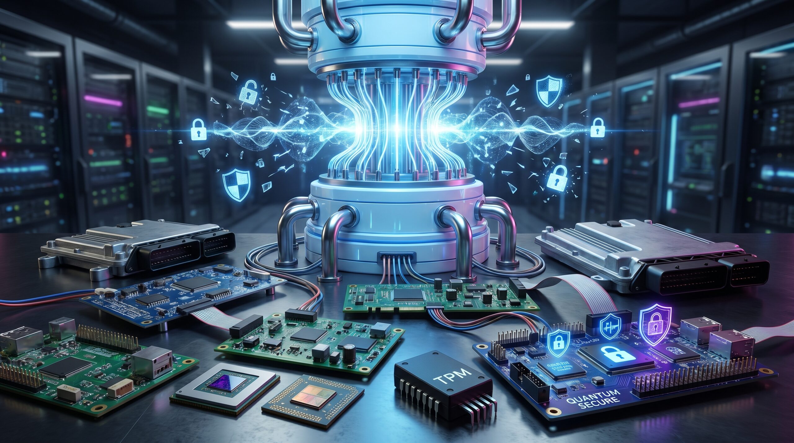
Is Your TPM Actually Ready for Post-Quantum Cryptography?
(TPM = Trusted Platform Module — the security chip acting as hardware root of trust)
To be honest, this is the part I find most frustrating. The vendor announcements sound good. The reality under them isn’t.
The Trusted Computing Group released TPM 2.0 Library Specification v1.85 in March 2026, adding formal support for ML-KEM (FIPS 203) and ML-DSA (FIPS 204). WolfSSL shipped firmware TPM support for v1.85 on Cortex-M33 and STM32 secure enclaves. STMicroelectronics shipped the ST33KTPM with field-upgrade capability for PQC algorithms — authenticated via LMS signatures per NIST SP 800-208. Real progress.
But here’s what those announcements don’t say.
v1.85 is from March 2026. The chips implementing it are new. The TPM 2.0 chips soldered onto motherboards, sitting inside industrial panels and medical enclosures around the world right now? Earlier specs. Fixed algorithm sets. Defined in silicon. ML-KEM and ML-DSA not included.
Field-upgradeable firmware TPMs exist — but only if the chip was built for it, if the OEM supports the signed update, and if the host secure boot chain can authenticate the new payload. Most TPMs shipped before v1.85 don’t meet those conditions. Some enterprise-grade TPMs on programmable secure elements can get firmware updates — but that depends on NVM capacity and ongoing manufacturer support, conditions that narrow fast. Many discrete TPM architectures were not designed for field-upgradeable algorithm agility.
I know what you’re thinking — “but our vendor said migration is supported.” Maybe. Ask them specifically: which TPM revision is on your boards, does their support cover your product’s replacement lifecycle, and what happens if they drop support. I’ve noticed those three questions change conversations quickly.
A post-quantum TPM spec doesn’t help a device that shipped with a pre-v1.85 chip and no upgrade path. Many of those devices may ultimately need hardware replacement for native PQC support.
For non-engineers: think of it like a safe with a lock that can never be changed. New technique breaks the lock? Can’t retrofit. Buy a new safe. Most deployed TPMs are exactly that safe.
FPGA Bitstream Security and the Post-Quantum Gap Nobody Discusses
(FPGA = Field-Programmable Gate Array — a reprogrammable chip in telecom, defense, industrial systems)
I’ve found FPGAs get walked past in almost every post-quantum cryptography embedded systems migration conversation. That’s a mistake.
FPGAs use bitstream encryption to keep configuration images from being read, copied, or reverse-engineered. Most vendors use AES-256 for this. AES-256 is quantum-resilient — drops to roughly 128-bit effective security under Grover’s Algorithm, which cryptographers still consider solid. So that part’s fine.
The problem is how the AES key gets loaded. Full stop.
AMD (Xilinx) and Intel (Altera) — the two main FPGA vendors — both use RSA-based authentication as part of their key delivery architecture. Per AMD’s app note XAPP1267 (Encrypting and Authenticating eFUSE Programming for UltraScale and UltraScale+ FPGAs), UltraScale devices store the AES-256 key in BBRAM or eFUSE, with RSA auth verifying the boot image. AMD’s Security Bulletin AMD-SB-8002 (CVE-2023-20570) confirms RSA is structural to the boot authentication chain. Intel’s Quartus Prime Pro security docs describe the same RSA-based auth for Agilex and Stratix 10.
RSA is exactly what Shor’s Algorithm breaks. That’s the problem.
One caveat — good news if you’re designing new hardware: some 2024 and 2025 FPGAs use Physically Unclonable Functions (PUFs) for root key derivation. PUFs derive the AES key from physical manufacturing variation rather than BBRAM or eFUSE. Different threat model. If you’re doing a new design, look at FPGA families with PUF-based secure boot. But most FPGAs in the field — automotive, industrial, defense — predate PUF adoption. Those carry the RSA-layer exposure.
The bitstream is protected by AES-256. RSA authentication wraps the chain that provisions and controls that AES key. When a quantum computer breaks RSA, the whole boot and key-delivery chain is compromised — not because AES-256 failed, but because the layer above it did.
Plain version: the safe is strong. The key to the safe is in a box a quantum computer can open. Once they have the key, the safe doesn’t matter.
Per Semiengineering’s analysis citing Flex Logix engineering leadership, automotive and industrial chipmakers need to plan for ten to twenty-year device lifespans. Design quantum-safe key delivery before the first board spin. Not after.
What a Quantum-Aware Board Design Actually Takes
I’ve found NIST, NSA, and NCSC guidance is solid at the algorithm level. What’s missing is the translation down to the board. Here it is.
Inventory at the component level — not the software level. Every chip. Every TPM. Every secure element. Every FPGA. Mapped against silicon algorithm support and upgrade path. A Cortex-M0+ running ECDH for IoT auth is a completely different post-quantum cryptography embedded systems migration problem from a server-side TLS stack. Both need to move. Neither moves the same way. Do the inventory first.
SRAM budget before algorithm. ML-KEM-512 needs 5.1–6.7 KB total RAM per arXiv:2603.19340 preprint data. ML-DSA needs 8.4–8.9 KB. On a device with 8 KB total SRAM, those are hard stops — not optimization targets. If the chip can’t fit the lowest PQC parameter set, the path is hardware replacement. That decision belongs on the plan now.
Secure boot is the critical path. The chain from hardware root of trust through bootloader through firmware is where transitions get ugly. Mask ROM is immutable. RSA-2048 verification burned into mask ROM means no patch — only a hardware respin. Know which layers are immutable before designing the migration timeline.
Side-channel exposure in PQC implementations — don’t skip this. ML-KEM and ML-DSA introduce new side-channel surfaces: power analysis during NTT (Number Theoretic Transform) ops, EM leakage during polynomial multiplication, timing variance from ML-DSA rejection sampling. For medical devices, automotive ECUs, defense electronics — migrating without evaluating the side-channel profile is an incomplete migration. PSA Certified Level 2 and SESIP (Security Evaluation Standard for IoT Platforms) are the right frameworks.
Crypto-agility on the next board spin. Devices shipping today will be in the field through the quantum transition. The next spin needs PQC as a first-class silicon requirement: SRAM headroom for ML-KEM and ML-DSA buffers, a TPM with a v1.85-capable upgrade path, FPGA key delivery built around ML-KEM transport, and a secure boot chain that authenticates ML-DSA or LMS-signed firmware per NIST SP 800-208.
The Hardest Part — What’s Already in the Field
I want to be direct about this. It’s uncomfortable.
Hundreds of millions of embedded devices are running right now — hospitals, power grids, factory floors, cars — on RSA and ECC hardware that can’t migrate to ML-KEM. Some have ten-year windows. Some fifteen. Some will outlast the 2035 federal migration planning horizon per NIST guidance and the EU Cyber Resilience Act’s IoT security-update requirement.
Per RAND Corporation’s 2023 assessment of quantum computing vulnerabilities in ICS and OT environments (RR-A2427-1), hardware replacement cycles are measured in decades, and operational constraints make taking critical infrastructure offline essentially impossible.
To be honest, the migration plan for those devices isn’t about algorithms. It’s end-of-life planning, network segmentation, and formally documented risk acceptance — in that order. The conversation isn’t just “which algorithm.” It’s “which devices are stuck, and what’s the risk posture until they can be replaced.”
That conversation needs someone who knows what’s actually on the board.
Not just what’s in the deck.
This is Part 2 of a two-part series. Read Part 1: [The Quantum Computer Is Coming: Why Today’s Encryption Could Soon Be Useless] for the foundational overview — RSA, ECC, HNDL attacks, and the NIST PQC standards.
About the Author
Imran Valiani | Sales Director, PCB Electronics Manufacturing — 20+ years working with major Bay Area and global tech clients. Founder of Silicon to Software, where I write about the hardware layer — PCB fab, AI gear, autonomous systems, and cyber — the stuff most tech writers have never touched. Literally. Follow: X @SiToSoftware | LinkedIn
This post was written with AI assistance. See my full AI disclosure.
Sources & Further Reading
NIST FIPS 203, Table 2, August 2024
NIST FIPS 204, Table 1, August 2024
NIST FIPS 205, August 2024
arXiv:2603.19340 (preprint), Chhetri, “Benchmarking NIST-Standardized ML-KEM and ML-DSA on ARM Cortex-M0+: Performance, Memory, and Energy on the RP2040,” March 2026
Kannwischer et al., “pqm4: Testing and Benchmarking NIST PQC on ARM Cortex-M4,” NIST PQC Conference, 2019
wolfSSL, “Benchmarks for Kyber Level 1 PQM4 Integration on STM32,” wolfssl.com
AMD XAPP1267, Encrypting and Authenticating eFUSE Programming for UltraScale and UltraScale+ FPGAs
AMD Security Bulletin AMD-SB-8002 (CVE-2023-20570)
Intel Quartus Prime Pro Edition Security Overview for SDM-based FPGA Devices
Trusted Computing Group, TPM 2.0 Library Specification v1.85, March 12, 2026
wolfSSL, “The First Firmware TPM with Post-Quantum Cryptography,” 2026
STMicroelectronics ST33KTPM product page
NIST SP 800-208, October 2020
NIST IR 8547, 2024 initial public draft
NIST SP 800-56C Rev. 2
NSA Cybersecurity Advisory, CNSA 2.0, September 202
RAND Corporation, RR-A2427-1, October 2023
EU Cyber Resilience Act
NIST PQC migration guidance
Flex Logix, cited in the Semiengineering analysis
PSA Certified — psacertified.org
GlobalPlatform SESIP specification — globalplatform.org
STMicroelectronics STSAFE-A, Microchip ATECC, NXP SE050 product lines